Hi folks !
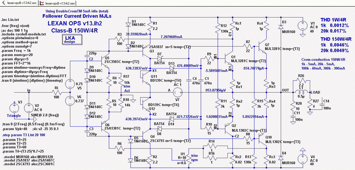
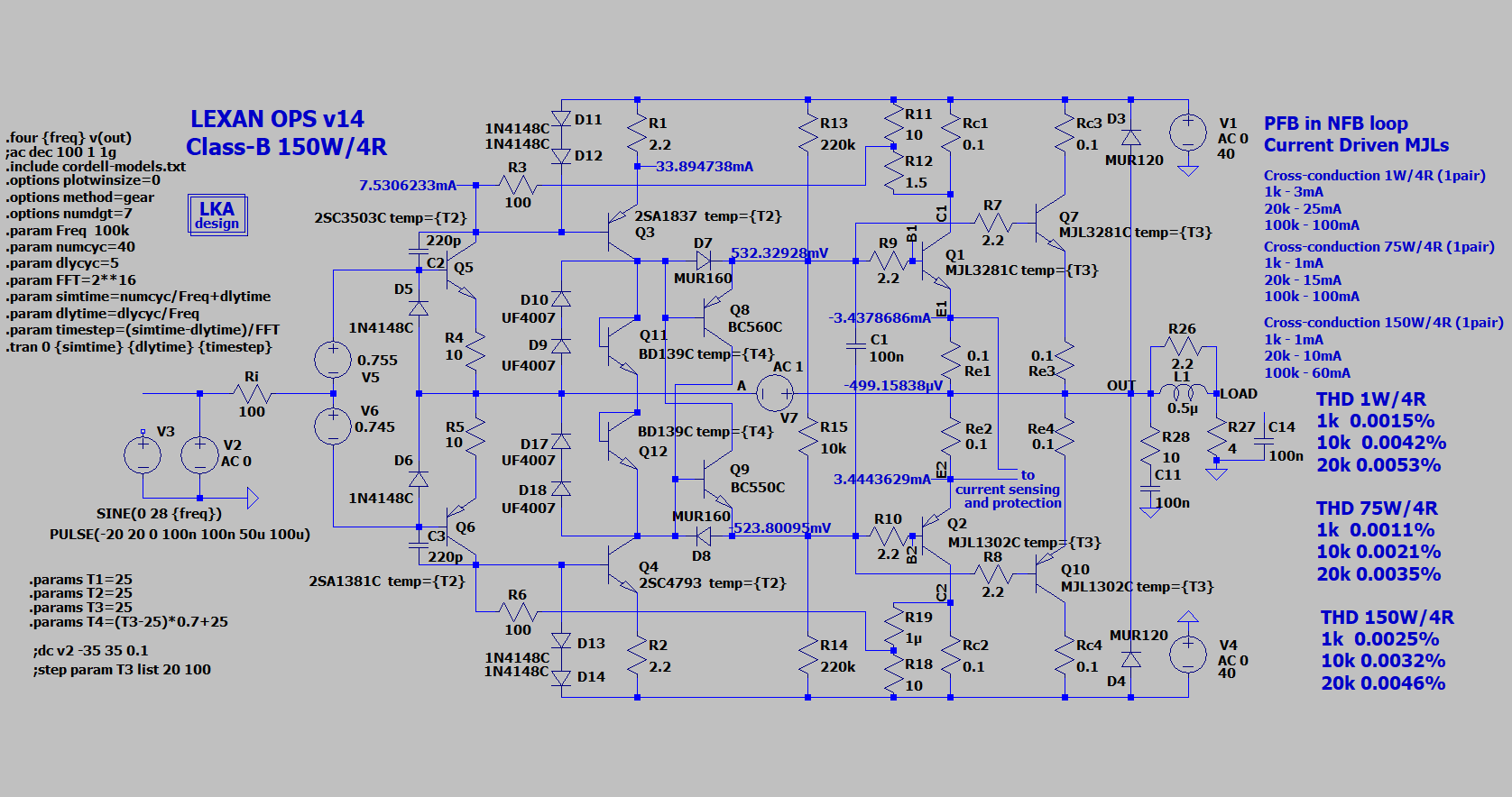
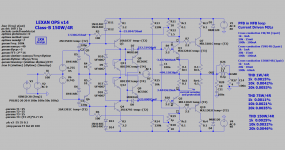
A couple of months ago I read Ian Hegglun article about current driven OPS (Linear Audio vol 13). At this time I came across an interesting Class-B amplifier modified by local member Danhard on czech forum. He also improved the old texan amp and helped me to create this output stage which main features are:
* Class-B, 150W/4R, idle current < 1mA
* Current driven output transistors
* voltage gain 1
* Positive feedback in NFB loop
* distortion < 0.01% (1-150W/4R,20-20kHz)
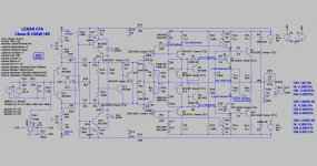
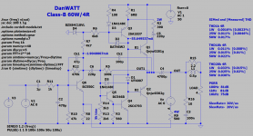
The following schematic diagram is not final, it was never build, maybe has serious errors, etc.
I'm publishing it for further discussion in a hope we'll able to improve it.
Ian gave me some helpful advice already, thanks. And of course the czech guru Danhard, vdaka fesak.
A couple of months ago I read Ian Hegglun article about current driven OPS (Linear Audio vol 13). At this time I came across an interesting Class-B amplifier modified by local member Danhard on czech forum. He also improved the old texan amp and helped me to create this output stage which main features are:
* Class-B, 150W/4R, idle current < 1mA
* Current driven output transistors
* voltage gain 1
* Positive feedback in NFB loop
* distortion < 0.01% (1-150W/4R,20-20kHz)
The following schematic diagram is not final, it was never build, maybe has serious errors, etc.
I'm publishing it for further discussion in a hope we'll able to improve it.
Ian gave me some helpful advice already, thanks. And of course the czech guru Danhard, vdaka fesak.
Last edited:


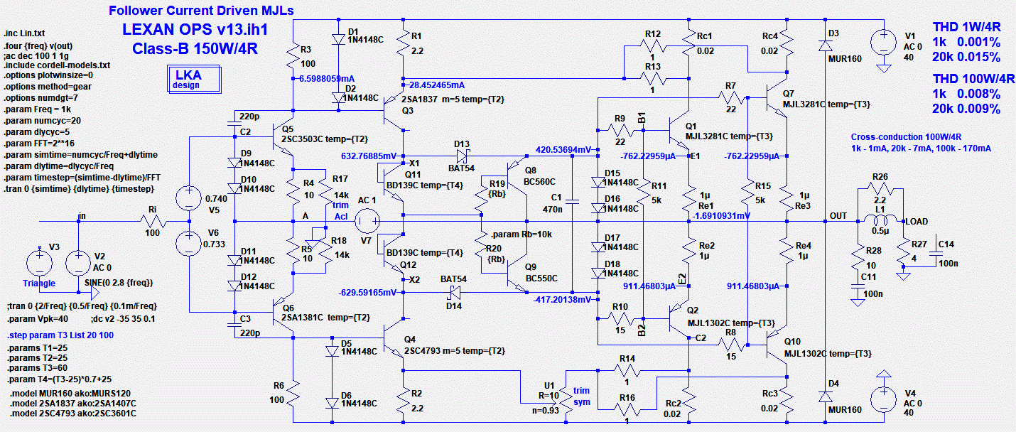
Low distortion current driven Class-B output stage mods
Thanks for posting the LTspice sim file. This method has potential. Very few successful amplifiers have used it, possibly because it is not easy to do it.
I have tried a lot of things: to get the bias stable without emitter resistors and paralleling, and ensure negligible cross-conduction at 100kHz, and for minimal crossover gain spikes using a very low idle current (just a few mA).
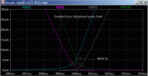
Two circuits are attached. An explanatory text file is attached giving my changes. A DoubleCross version is shown below
It significantly reduces the crossover gain blip with two displaced pairs in parallel as shown below

.
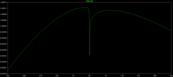
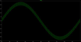
A single stage when current driven and biased with 0.5mA gives a significant gain glitch from delayed turn on due to slow removal of stored base charge in the turning off transistor, see below

.
Notice the huge gain glitch. With DoubleCross this is glitch is hardly visible (run the attached circuit if you want to see it).
Although the glitch is squashed using DoubleCross, the THD readout doesn't reduce much because its energy gets spread over a slew of high order harmonics that don't add to much when RMS summed. But they need to be reduced because we often hear these high order harmonics (when they fall in the 300Hz-3kHz region.
That's why THD figures from this type of distortion does not correlate very well with sound quality. Weighting distortion harmonics helps to correlate better with sound quality. It is not hard to do.
For more on on OPS current drive advantages and disadvantages etc read the attached txt file. A free snippet PDF from my LA V13 current drive amp is here Class AB+C: Anybody tried it? Is it worth it?
-------
Future:
The input stage still needs bias generators to make and test it.
The driver stage may need some temperature compensation.
Edit: Oops, the schematics don't show the 8 current limit diodes (removed for clarity). There should be a pair of 1N4148's on each node of C1 and C4, like on the input stage with their centre to "out". This limits the output current to 10A (for basic SOA) and the NPN base resistors are slightly larger than the PNP due to higher Beta of the NPN's.
Cheers,
Ian Hegglun
Hi Ladislav,I'm publishing it for further discussion in a hope we'll able to improve it.
Thanks for posting the LTspice sim file. This method has potential. Very few successful amplifiers have used it, possibly because it is not easy to do it.
I have tried a lot of things: to get the bias stable without emitter resistors and paralleling, and ensure negligible cross-conduction at 100kHz, and for minimal crossover gain spikes using a very low idle current (just a few mA).
Two circuits are attached. An explanatory text file is attached giving my changes. A DoubleCross version is shown below
It significantly reduces the crossover gain blip with two displaced pairs in parallel as shown below
.
A single stage when current driven and biased with 0.5mA gives a significant gain glitch from delayed turn on due to slow removal of stored base charge in the turning off transistor, see below
.
Notice the huge gain glitch. With DoubleCross this is glitch is hardly visible (run the attached circuit if you want to see it).
Although the glitch is squashed using DoubleCross, the THD readout doesn't reduce much because its energy gets spread over a slew of high order harmonics that don't add to much when RMS summed. But they need to be reduced because we often hear these high order harmonics (when they fall in the 300Hz-3kHz region.
That's why THD figures from this type of distortion does not correlate very well with sound quality. Weighting distortion harmonics helps to correlate better with sound quality. It is not hard to do.
For more on on OPS current drive advantages and disadvantages etc read the attached txt file. A free snippet PDF from my LA V13 current drive amp is here Class AB+C: Anybody tried it? Is it worth it?
-------
Future:
The input stage still needs bias generators to make and test it.
The driver stage may need some temperature compensation.
Edit: Oops, the schematics don't show the 8 current limit diodes (removed for clarity). There should be a pair of 1N4148's on each node of C1 and C4, like on the input stage with their centre to "out". This limits the output current to 10A (for basic SOA) and the NPN base resistors are slightly larger than the PNP due to higher Beta of the NPN's.
Cheers,
Ian Hegglun
Attachments
Ian, thanks for your contribution.
I noticed one thing. You've removed the switch-off circuit (Q8,Q9 are activated at higher power level only) and completely relied on switch-off capacitors. But with this, after several cycles the capacitor voltage rises and significant cross-conduction happens.
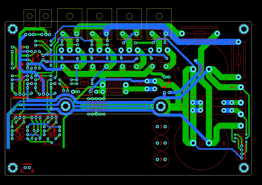
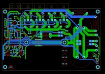
Meanwhile I'm working on the pcb design, only the front-end part is missing ...
Cheers, L
I noticed one thing. You've removed the switch-off circuit (Q8,Q9 are activated at higher power level only) and completely relied on switch-off capacitors. But with this, after several cycles the capacitor voltage rises and significant cross-conduction happens.
Meanwhile I'm working on the pcb design, only the front-end part is missing ...
Cheers, L
Attachments
Last edited:
Oops - updated circuits attached
Hi Ladislav,
Ops, I completely missed noticing that slow rise in cross conduction😱.
Attached are the files with Q8 and Q9 back in.
BTW I still use some positive feedback to trim the PNP gain up to the NPN (best seen with dc v2 -35 35 0.1
I found too much positive feedback can cause the driver transistors to not cutoff with large input swing (seen plotting I(Q3) in your original circuit) - undesirable cross-conduction in the driver. An alternative is to add resistors to R4 and R5 to common, this reduces the feedback factor slightly below 100% which increases the closed loop voltage gain, same as using positive feedback, but without cross-conduction in the driver.
Some positive feedback to trim the PNP gain up to the NPN makes a big difference so the 2nd harmonic, my aim is to reduce it below the 3rd so it does not dominate in the THD values.
Also a few percent over-unity gain in the output stage can increase the amps output swing from the VAS.
I hope you find some of my suggestions useful. Don't feel obligated to use them. Maybe other members can find something useful here too.
BTW what IPS do you have in mind. PM me if you prefer.
Cheers,
IanH
Ian, thanks for your contribution.
... after several cycles the capacitor voltage rises and significant cross-conduction happens.
Hi Ladislav,
Ops, I completely missed noticing that slow rise in cross conduction😱.
Attached are the files with Q8 and Q9 back in.
BTW I still use some positive feedback to trim the PNP gain up to the NPN (best seen with dc v2 -35 35 0.1
I found too much positive feedback can cause the driver transistors to not cutoff with large input swing (seen plotting I(Q3) in your original circuit) - undesirable cross-conduction in the driver. An alternative is to add resistors to R4 and R5 to common, this reduces the feedback factor slightly below 100% which increases the closed loop voltage gain, same as using positive feedback, but without cross-conduction in the driver.
Some positive feedback to trim the PNP gain up to the NPN makes a big difference so the 2nd harmonic, my aim is to reduce it below the 3rd so it does not dominate in the THD values.
Also a few percent over-unity gain in the output stage can increase the amps output swing from the VAS.
I hope you find some of my suggestions useful. Don't feel obligated to use them. Maybe other members can find something useful here too.
BTW what IPS do you have in mind. PM me if you prefer.
Cheers,
IanH
Attachments
Driver local NFB
Hi All,
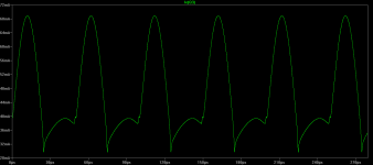
Local negative feedback via the driver seems to improve the crossover region.
.
The attached file includes a DoubleCross version giving crossover lower distortion with 6mA idle total (compared to 2mA total without DoubleCross).
Hi All,
Local negative feedback via the driver seems to improve the crossover region.
.
The attached file includes a DoubleCross version giving crossover lower distortion with 6mA idle total (compared to 2mA total without DoubleCross).
Attachments
Hi Ladislav,your suggestions are very useful
I'd like to use simple front-end (not much space left on the pcb) like this one. It looks quite stable.
Thanks. You circuit looks similar to one I was helping AndryOL early 2018; IIRC the last circuit was Post 775 in this thread here One of the Top Solid-State CFA amp design and I believe it was based on a LazyCat amp.
AndryOL's output stage is a 3 stage CFP like yours except for the current drive of the MJL's. And similar IPS and VAS to yours.
His sims showed 0.0003% THD at 20kHz with Dadod's OITPC like compensation. Impressive if he can get close to that in real life.
Last I heard from AndryOL's early this year it isn't built and tested yet. My sims showed his OPS was tricky to get it to survive a 100kHz full output swing test without overheating the drivers.
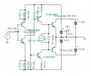
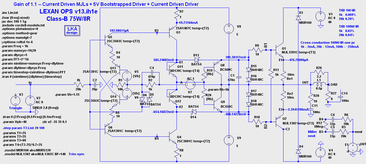
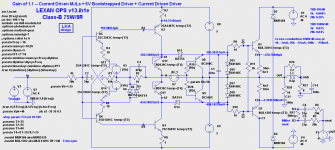
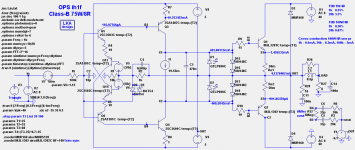
Gain of 2 version with a current driven driver stage
Hi Ladislav,
Using Rush pairs in the input stage allows a gain of 2 with low power feedback resistors as well as nulling out the PNP-NPN offset voltage of the input transistors. A gain of 2 reduces the swing from the VAS so lower VAS distortion and no need for boosted rails.
Also, a standard voltage opamp with +/-18V rails can drive this amp to full output. One way to simplify an input stage.

Notice the driver transistors (Q3,Q4) are now current driven. This makes better use of the driver's Beta and lowers the input stage base current. It also lowers the gain since the driver stage works at much lower current. That can explain why THD readings are higher than my previous circuits. Using a gain of 2 doubles THD readings for a start.
For current drive of the driver transistors I use some Miller neutralization to speed up turn off for operation up to 100kHz without too much cross conduction. A 5Meg resistors across B3 and B4 keeps Q3 and Q4 on slightly (about 1mA) with large swings.
Another advantage of low input stage current is the ability to null out most of the 3rd harmonic by trimming the input stage bias (not possible in earlier circuits). Unfortunately, MJL Beta differences cannot now be trimmed with feedback from the MJL collector resistors (since feedback cannot be sent via the driver transistors anymore under current drive). There may be another method to trim out Beta asymmetry? Suggestions anyone?
The attached file also includes a DoubleCross version.
Just more ideas to mull over. Probably most have not seen these ideas before.
Hi Ladislav,
Using Rush pairs in the input stage allows a gain of 2 with low power feedback resistors as well as nulling out the PNP-NPN offset voltage of the input transistors. A gain of 2 reduces the swing from the VAS so lower VAS distortion and no need for boosted rails.
Also, a standard voltage opamp with +/-18V rails can drive this amp to full output. One way to simplify an input stage.
Notice the driver transistors (Q3,Q4) are now current driven. This makes better use of the driver's Beta and lowers the input stage base current. It also lowers the gain since the driver stage works at much lower current. That can explain why THD readings are higher than my previous circuits. Using a gain of 2 doubles THD readings for a start.
For current drive of the driver transistors I use some Miller neutralization to speed up turn off for operation up to 100kHz without too much cross conduction. A 5Meg resistors across B3 and B4 keeps Q3 and Q4 on slightly (about 1mA) with large swings.
Another advantage of low input stage current is the ability to null out most of the 3rd harmonic by trimming the input stage bias (not possible in earlier circuits). Unfortunately, MJL Beta differences cannot now be trimmed with feedback from the MJL collector resistors (since feedback cannot be sent via the driver transistors anymore under current drive). There may be another method to trim out Beta asymmetry? Suggestions anyone?
The attached file also includes a DoubleCross version.
Just more ideas to mull over. Probably most have not seen these ideas before.
Attachments
Bootstrapped supplies for IPS+drivers?
That's an interesting circuit. I have adapted it to Ladislav's with my Rush version. Two versions are attached. The first uses a current source between the bases to absorb 99% of the driver current ("f" version).

.
The other "e" version uses diodes and base charge pull-out transistors.
.
With bootstrapped rails for the IPS and driver a high input resistor and small input capacitor is needed to stop it oscillating. Also the gain cannot be set more than 10% above unity with 5V supplies.
The advantage of supply bootstrapped rails for the IPS and driver are lower dissipation and low voltage devices which are more common and faster than HV transistors. It appears to increase the driver output resistance for better current drive but this does not seem necessary (with biasing in the mA range) or helpful since distortion is not reduced but increased with bootstrapping and it is harder to get stable. Maybe the Rush stage make stability more difficuly, so the blame may not be entirely with supply bootstrapping.
After trying many variants I am warming to the idea of feedforward correction (eg current dumping) to fill in the missing part (from the base charge delay notch). Since none of the variants tried so far are effective at fixing the crossover region with idle currents in the sub mA range for 100W plus amps. DoubleCross seems to be the next best option to current dumping IMO.
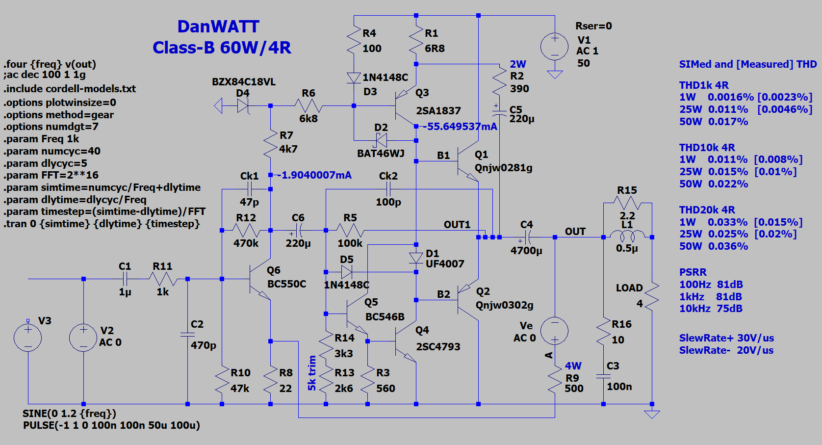
Hi kokoriantz,Maybe this topology can be useful for you. It is biased 4ma and relies on Hfe thermal variation which is acceptable. It doesn't have so low distortion numbers but your measurement with 100 ohms source impedance is not realistic .
That's an interesting circuit. I have adapted it to Ladislav's with my Rush version. Two versions are attached. The first uses a current source between the bases to absorb 99% of the driver current ("f" version).
.
The other "e" version uses diodes and base charge pull-out transistors.
.
With bootstrapped rails for the IPS and driver a high input resistor and small input capacitor is needed to stop it oscillating. Also the gain cannot be set more than 10% above unity with 5V supplies.
The advantage of supply bootstrapped rails for the IPS and driver are lower dissipation and low voltage devices which are more common and faster than HV transistors. It appears to increase the driver output resistance for better current drive but this does not seem necessary (with biasing in the mA range) or helpful since distortion is not reduced but increased with bootstrapping and it is harder to get stable. Maybe the Rush stage make stability more difficuly, so the blame may not be entirely with supply bootstrapping.
After trying many variants I am warming to the idea of feedforward correction (eg current dumping) to fill in the missing part (from the base charge delay notch). Since none of the variants tried so far are effective at fixing the crossover region with idle currents in the sub mA range for 100W plus amps. DoubleCross seems to be the next best option to current dumping IMO.
Attachments
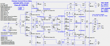
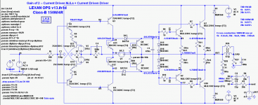
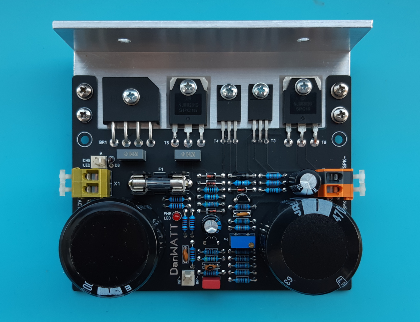
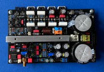
Current driven amplifier capability demonstration. It's an retro thing in a new coat. Its roots are in 60s (RCA Power Circuits 1969, p402). The czech tranziwatt modded by Danhard, built by myself. Amazing to see that simple circuit performance.
Attachments
Last edited:
Hi LKA,Current driven amplifier capability demonstration. It's an retro thing in a new coat. Its roots are in 60s (RCA Power Circuits 1969, p402). The czech tranziwatt modded by Danhard, built by myself. Amazing to see that simple circuit performance.
Very nice PCB and assembly work! You are a mistro.
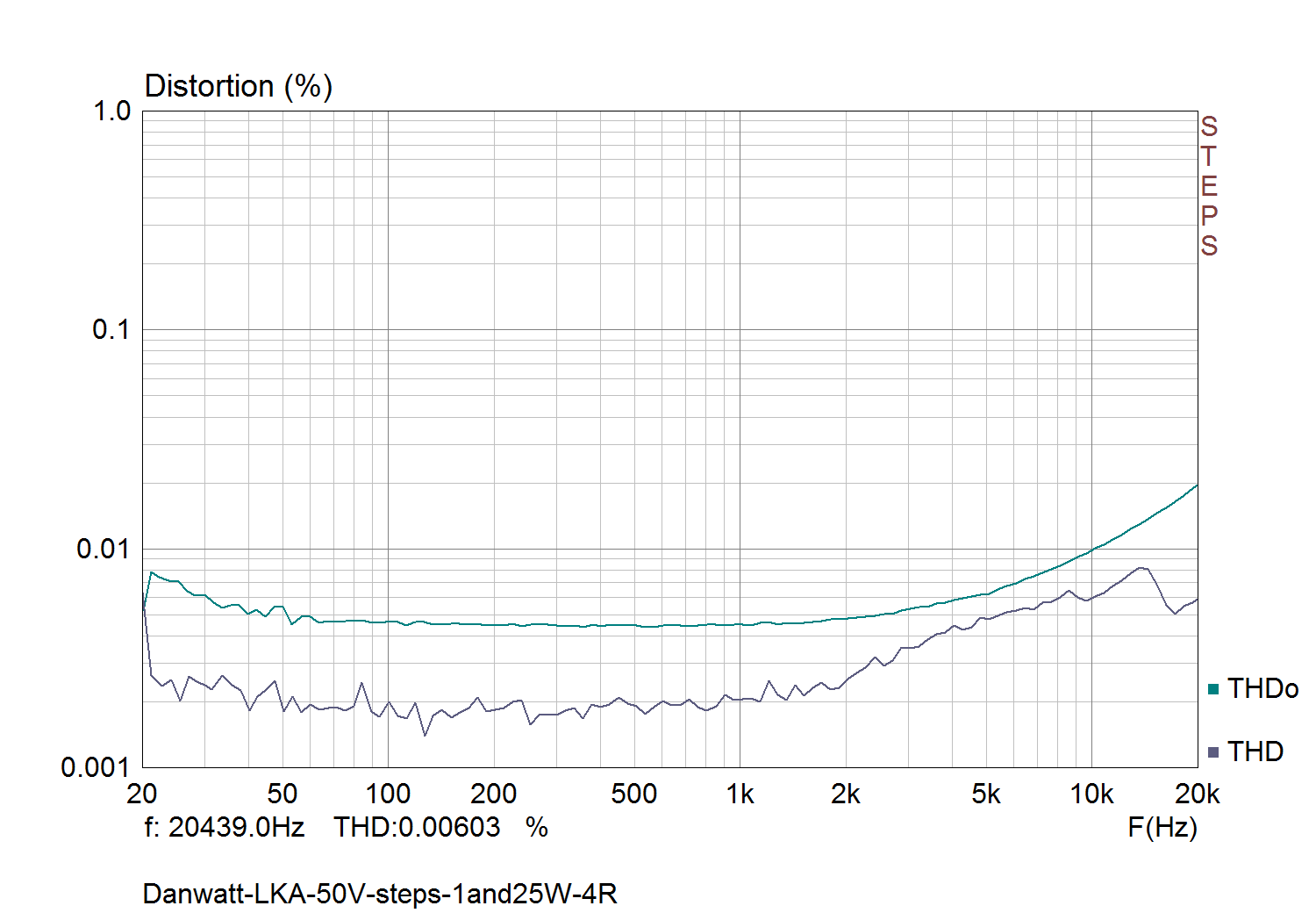
This "retro" circuit has only one bias diode between the OPS bases so must be less than 1mA bias for "Class-B" mode. The THD measures fairly close to simulated which is a good reality check for simulations.
Have you listened carefully to it? If so what sensitivity speakers are you using? Speaker sensitivity can make a world of difference to how different amps sound, strange as that may sound🙂.
BTW I simulated some feedbforward circuit variations for your Lexan. Shall I post them? Or are you overloaded with variants?
Singleton input amps have warm, dark and soft sound with huge soundstage. I would recommend them with excessively bright loudspeakers or mini monitors like Proac Tablette. I would not recommend them with big floorstanders.
PCB is very nice and practical. Only transformer is needed, couple of connectors and enclosure.
PCB is very nice and practical. Only transformer is needed, couple of connectors and enclosure.
Hi, almost done, some components still on the way, I can't wait.


An externally hosted image should be here but it was not working when we last tested it.
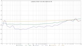
The prototype measurement: 1W,10W,100W into 4R
Rails: +-41V at idle
Clip : 140W/4R
Slew rate : 50V/us
Idle currents:
driver - 25mA
outputs - 1mA/pair, 2mA total
module total - 55mA
still under development and tuning
Rails: +-41V at idle
Clip : 140W/4R
Slew rate : 50V/us
Idle currents:
driver - 25mA
outputs - 1mA/pair, 2mA total
module total - 55mA
still under development and tuning
Attachments
Last edited:
Singleton input amps have warm, dark and soft sound with huge soundstage. I would recommend them with excessively bright loudspeakers or mini monitors like Proac Tablette. I would not recommend them with big floorstanders.
😕 This is generalisation...
- Home
- Amplifiers
- Solid State
- Low distortion current driven Class-B output stage