And it even comes in easily hand-solderable SOIC! Great, I'll keep that in mind for the distortion analyzer section.
I can't judge the details, but your description reads like there is a chance for trouble. Think about what currents flow into the ground plane, and how they return to the power supply. With most peak level detectors, there is significant current (dozen of mA) with very high harmonic content (THD possibly several dozen %) dumped into ground. If this current is allowed to flow through the main oscillator section, there's little chance that this would not result in drastic THD increase (even if this path is a solid low Z ground plane). My first dual sample-and-hold board years back introduced nice short spikes in the distortion residual of the oscillator output--perfectly aligned with the timing signals of the two sample-and-hold stages, and orders of magnitude higher than any other distortion source.
There are several means how you can avoid this trap (in order of importance, as far as I can tell):
* Good placement of the various oscillator subcircuits. Place the level detector between main oscillator circuitry and power supply entry. This will reduce the common return impedance coupling as the level detector return current will tend to flow back directly to the supply, and thus doesn't touch the main oscillator ground plane section.
* Use a local shunt supply for the most offensive sources (often the timing generators)--e.g. the AP System One uses an extra resistor-5 V zener-cap supply for the level detector logic rather than the already available 5 V rail. I recall that the SG505 has some heavy RC filtering in the peak detector as well, which is effectively some sort of AC shunt supply.
* Use ground plane slots to form individual return current sections. Of course no signal/supply trace may cross the slot.
There's of course also capacitive and inductive crosstalk going on, but with sufficient spacing this should not be drastic, usually.
Samuel
Hi Samuel,
The boards are laid to your description short of the ground plane slots. The AGC is on a separate board from the main oscillator. The only digital on the main oscillator board is the tuning Mdac's and digital is only active during a frequency change. All noisy and current hogging component are closest to the power entry or routed away from sensitive components on both boards. The only exception is the lamp drivers but these are part of the multiplier. The input to the lamp drivers is at the bottom left.
I can't see from the posted spectrum any sign of significant trouble. If there was the distortions would be a lot higher.
This distortion I speak of only occurs if I allow the input signal to the ADC to go negative. The clamping diodes in the ADC input cause significant current draw and this is the source of the gross distortion or a t least part of it. I can't imagine the 1468 liking this kind of sudden low Z load on it's output. It's likely a break out of parasitic oscillation in the 1468. It's simply not good practice to force an ADC outside it's range.
The +/- 25V rating is just a protection rating not an operation range. The actual range I configured is 0 - 5Vp. This is an industrial part and must be able to take punishment.
It has to be able to operate in harsh environments. I'm not at all concerned about increased distortion from over driving components. Besides I think I exaggerated the amount. You can go back a few post and look at the spectrum of various frequencies all at 3Vrms output.
I know it's difficult with out a schematic and parts designator description but you can look over the board here:
http://www.diyaudio.com/forums/digital-source/185761-open-source-usb-interface-audio-widget-216.html and tell me if you see something.
The board on the left is the oscillator, multiplier, lamp drivers and tuning Dacs.
The Dacs are at the top, oscillator middle, multiplier below left side and lamp drivers left bottom. On the right of the multiplier is the tuning caps. Power entry in on the top left side. Just above that is a 5V regulator for the Mdacs and above that is the SPI entry. Power is distributed by rails on the left. Positive on one side and negative on the bottom side. Sinal output is on the middle right of the board and below that is header pins for tuning jumpers.
The AGC board I have flipped around so the bottom in the pic is the top. I'll explain it as it's seen.
Bottom left is the power entry. Just above that is the highest current demand and noisiest component on the board. The zero crossing detector comparator. Beside that is a voltage regulator which supplies the comparator and input buffer to the comparator. The buffer is LP filtered with a 22 ohm and 10uF cap on each power pin.
The input buffer are on the bottom right. The ADC conditioner is power by the +/- 15V supply and LP filtered on the power pins. On the bottom right most is the signal entry 0/90 deg. On the left above the comparator is another 5V regulator supplying the cmos mono and ADC. The ADC is in the middle. On the left of the ADC is the analog references and filtering. Above the ADC is the Mdac, I/V convertor, integrator and summing amp. The error output is on the top right of the board. There is a couple of component at the top of the board that are not used, not needed but there for experimental purposes.
There is a single top ground plain. I may add filtering at the power entry.
If you want to see the bottom of the board I can send you some pics of the artwork.
Cheers,
Is there a reason to use a sample and hold instead of a track and hold?
There is no droop induced ripple on the output and I think there is less spiky noise generated. It does it all in one shot. Other than that it's just a different way of doing it with fewer components. Cost wise about the same if you use expensive switches.
I noted you mentioned two stages so I am sure you understand the difference, but for the others allowing more acquisition time reduces the surge currents.
Yes I saw this when I evaluated the THSH. The feed through is greatly reduced as well with cascade sections even if they sample synchronously.
If you look at the droop specs the S&H will need refreshing pretty often. Probably faster with higher temperature.
There is no reason why the AGC even needs to share much of a ground with the oscillator. A differential input monitoring the reference output node should be all that is necessary to get the level to the detector circuitry. For this application you need two, one for each phase to capture the zero crossing to trigger the sample. For absolute accuracy you may need adjustments to align the sample pulse with the peak. If its late or early there will be a drop as the frequency increases.
The S&H is refreshed every cycle. The Dac will hold the value indefinitely as long as there is power.
Yes I'm well aware of this and this is one reason I don't like using a diode on the FB of an op amp. The diode introduce a significant amount of capacitance causing a misalignment as frequency increases. Shows up in spice runs too. Schotkey is among the worse for this.
I'd rather it just wasn't there so if I can limit the negative input voltage range some other way I will. I have the timing from the zero crossing detector and could use a switch at the ADC input.
look for Jim Williams' articles on sampling clamps for settling time measurements - may have usable ideas
Linear Technology app notes AN-74, 79, 120
or I may just not understand what you're doing
Linear Technology app notes AN-74, 79, 120
or I may just not understand what you're doing
A little simulation work on Scott's noscillator (Is this the correct term? Couldn't find the post again where the name was introduced...):
noscillator_SG_r1.pdf
noscillator_SG_freq_response_r1.pdf
This one is based on a state-variable filter. If the output is taken from the low-pass output, it has the advantage of providing higher harmonic attenuation (~50 dB for the 2nd harmonic in this case) than the Wien topology. Also the center frequency is easily tuned without placing a wiper contact resistance directly in the signal path (R3/R4 partially implemented as trimmer, with the wiper going to the inverting opamp input), and there are no significant common-mode issues in the amplifiers.
I don't have much intentions to persue this approach further for my own use, but if there's sufficient interest (and someone is willing to offer me a prototype PCB for my own evaluation) I might find the time to work out a full schematic and layout.
Samuel
don't know for sure but recalling long ago articles on op amp filter topologies, synthetic inductors, duplicating RLC filters it seemed one principle was more sections for higher Q reduced individual component sensitivity
using high gain/positive feedback to boost low passive network Q multiplies sensitivity - early on the bigger concerns were for op amp GBW effects
from that I would expect cascading multiple stages of biquad or state variable filters would lower component sensitivity
but maybe many concerns go away when you can have > 100x GBW op amps compared to filter center/corner, gain product today
still seems to me that the multiplied passive component sensitivity will be an issue with higher positive feedback/Q boosting of fewer passive sections - or of "differencing" schemes like twin T
Last edited:
A little simulation work on Scott's noscillator (Is this the correct term? Couldn't find the post again where the name was introduced...):
noscillator_SG_r1.pdf
noscillator_SG_freq_response_r1.pdf
This one is based on a state-variable filter. If the output is taken from the low-pass output, it has the advantage of providing higher harmonic attenuation (~50 dB for the 2nd harmonic in this case) than the Wien topology. Also the center frequency is easily tuned without placing a wiper contact resistance directly in the signal path (R3/R4 partially implemented as trimmer, with the wiper going to the inverting opamp input), and there are no significant common-mode issues in the amplifiers.
I don't have much intentions to persue this approach further for my own use, but if there's sufficient interest (and someone is willing to offer me a prototype PCB for my own evaluation) I might find the time to work out a full schematic and layout.
Samuel
Thanks, I figured either of the no common mode signal type circuits would work. Just more ideas for the mix.
I would like to see the full development of your design concept. Will help in what ever way is needed. We have a few ideas that have been tested and either completed or in the process towards completion with data shown along the way. Each a little different in approach from the other.
Thx-RNMarsh
Thx-RNMarsh
What's happening - progressing OK?
-RNM
Okay an update on development.
Firstly I don't have the level problems I thought I did.
Turns out it was a measurement error. My Fluke 8050A either need to be cal'ed or repaired. This was troubling me because I could see a peak level change.
I retested on the 339A and found the level to deviate, through three lower ranges, 0.01db to 0.02 db. That's not bad and more like it.
Secondly, I found the ADC clamping is not causing a rise in distortion. Because the input conditioning has a DC bias (reference) voltage on it, the signal is offset and at larger signal level the negative swing run into the rail and clips. No big deal to handle this. The distortion is not present at lower operating level 3Vrms. The conditioner only requires a small amount of clamping which shouldn't introduce any significant phase shift which might upset the level flatness.
The range of the multiplier is limited as it is and I can't get stable leveling to 100kHz. I can increase the range or use less decoupling but if it means an increase in distortion then I don't see the point of having the SVO go to 100kHz. As it is it can go to about 70kHz.
The next order of business is power supply/regulation, output amplifier/attenuator and control isolation.
New PCB design with the changes.
It will be a while
Cheers,
Last edited:
can you show a block diagram or similar of the distortion measuring system you are designing at this time?
[I can live with 70Khz]
Thx-RNM
[I can live with 70Khz]
Thx-RNM
can you show a block diagram or similar of the distortion measuring system you are designing at this time?
[I can live with 70Khz]
Thx-RNM
I don't have a distortion measurement system on the table. Just an SVO.
I Believe Samuel is working on an distortion analyzer.
I'll get back to the work on the ADC stuff once the SVO is done.
Cheers,
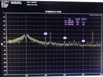
Once upon a time... when we were modifying an HP-339A for lower distortion, someone asked to see an FFT of the harmonics. here it is at 1 volt out/1 KHz out of the monitor port to the QA400 FFT. I just got this QA400 working on one PC -- I havent yet tried to see where the multiples of 2.25KHz are coming from but as you can see the harmonics from the 339A 1 KHz fundamental are labelled as MO (2H) etc. Note the 0 = -80dB full scale (I didnt do the x10 mod that davada did):
-138 and -148dB for 2H and 3H... ...
Thx-RNMarsh
-138 and -148dB for 2H and 3H... ...
Thx-RNMarsh
Attachments
Last edited:
Richard:
The way I capture the screen from the QA400 is to edit>copy bitmap to clipboard
switch to Paint Paste (the image from the clipboard) save as. . .PNG somewhere I can find the image and then upload that. Its quicker to do than to describe. A direct "save as" would be nice. This gets the full resolution and looks good when posted on the web.
The 2.5 KHz stuff may come from the USB interface. Its the common ground problem.
Once upon a time... when we were modifying an HP-339A for lower distortion, someone asked to see an FFT of the harmonics. here it is at 1 volt out/1 KHz out of the monitor port to the QA400 FFT. I just got this QA400 working on one PC -- I havent yet tried to see where the multiples of 2.25KHz are coming from but as you can see the harmonics from the 339A 1 KHz fundamental are labelled as MO (2H) etc. Note the 0 = -80dB full scale (I didnt do the x10 mod that davada did):
-138 and -148dB for 2H and 3H... ...
Thx-RNMarsh
Hi Rick,
I'm not clear about what you're measuring this on. Is it the monitor output of the 725?
No. I already did that earlier with 725 and an HP 3580A Spectrum Analyzer. This is from the monitor output of the HP 339A into the QA400.
[BTW - no one should expect this level of performance at all freqs... I tuned it down to near zero at 1KHz only --- 10 x 100 range/scale]
-RNM
[BTW - no one should expect this level of performance at all freqs... I tuned it down to near zero at 1KHz only --- 10 x 100 range/scale]
-RNM
Last edited:
Richard:
The way I capture the screen from the QA400 is to edit>copy bitmap to clipboard
switch to Paint Paste (the image from the clipboard) save as. . .PNG somewhere I can find the image and then upload that. Its quicker to do than to describe. A direct "save as" would be nice. This gets the full resolution and looks good when posted on the web.
The 2.5 KHz stuff may come from the USB interface. Its the common ground problem.
Thanks, Demian. I needed to know that... helps speed things along. What a pain in the butt.
-RNM
Last edited:
The range of the multiplier is limited as it is and I can't get stable leveling to 100 kHz. I can increase the range or use less decoupling but if it means an increase in distortion then I don't see the point of having the SVO go to 100 kHz. As it is it can go to about 70 kHz.
Didn't we discuss, some time back by e-mail, a simple means (pure C or a RC network in parallel with the input resistor of the inverting stage) to control the Q enhancing effect, as done in the SG505 and System One? At the time of writing, my oscillator design has a steady-state control voltage range of less than +/-1 V (of a maximum of about +/-12 V) from 10 Hz to 100 kHz, and that's with very low multiplier authority.
Once upon a time... when we were modifying an HP-339A for lower distortion, someone asked to see an FFT of the harmonics. here it is at 1 volt out/1 KHz out of the monitor port to the QA400 FFT. I just got this QA400 working on one PC--I havent yet tried to see where the multiples of 2.25 kHz are coming from but as you can see the harmonics from the 339A 1 KHz fundamental are labelled as MO (2H) etc. Note the 0 = -80 dB full scale (I didnt do the x10 mod that davada did):
-138 and -148 dB for 2H and 3H...
This is from the monitor output of the HP 339A into the QA400.
Not sure I follow. You're measuring the output of the modified 339A oscillator section by feeding it to the analyzer section of the 339A, and then the residual monitor output to the QA400?
Samuel
- Home
- Design & Build
- Equipment & Tools
- Low-distortion Audio-range Oscillator