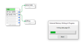
I have a 3e audio USBi link which is not recognized by sigma studio, it worked fine before a PC crash, can some post a link to the tcip -wifi software second edition, i have a 1466 DSP. TIA
I was reading that quite some people are having issues with these ADAU1452 boards.
This one in particular:
View attachment 1247466
Somebody on another forum also couldn't load any programs in.
Although it seems that the DSP is connected.
The following is worth a try (I don't have one of these boards atm, so can't test it by myself)
I have worked with these ADAU145x DSP's quite a bit in the past, so this reminded me of two things.
1 - either selfboot mode is not enabled
2 - EEPROM is not working properly (fails to write or something)
So I also found the GERBER view from the top layer online;
View attachment 1247467
According the datasheet, we are looking for pin 34 at the DSP IC:
So following the traces from pin 34, it goes trough the SIP1 header and than R7 to (I assume) 3V3.
So this part seems to be correct.
For the 2nd issue, we have to focus around IC5.
The write protect is on PIN7.
According to the datasheet of the EEPROM;
Pin7 from IC5 is connected to R120 and R121.
R120 is a resistor connected to 3V3.
However, R121 doesn't seem to be populated!
In other words, according to this picture and GERBER view, the EEPROM is in always write protect mode.
Shortening the pins of R121 will put the EEPROM in write mode, needed while writing.
Or one can just solder a little wire from the connection between R120+R121 to bottom leg of jumper CN5 (the one with the number "9" next to it).
According to the information I have, it seems they populated the wrong position, they should have populated IC7 instead, which is directly connected to the write protect jumper CN5.
No idea if this will solve problems, but purely on paper, this shouldn't work as it is now.
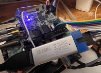
I have the same ADAU card.
everything works.
but I can't write on it, every time I turn it off it loses everything.
help!!!!!!!!!!!!!!!!!!!!
a question.
if I need 3 LEDs.... but 3 LEDs are already busy on the board, and exactly the MP11, MP12 and MP13 LEDs are already soldered.... and MP6, MP7 and MP9 are already busy as switches always on the board.. In this situation where do I connect my 3 LEDs? can I connect them in parallel to the LEDs on the board? (MP11, MP12, MP13)
if I need 3 LEDs.... but 3 LEDs are already busy on the board, and exactly the MP11, MP12 and MP13 LEDs are already soldered.... and MP6, MP7 and MP9 are already busy as switches always on the board.. In this situation where do I connect my 3 LEDs? can I connect them in parallel to the LEDs on the board? (MP11, MP12, MP13)
First time posting here, I thought I'd share my experience with programming the nvarcher v2 ADAU1452 board as snippets of a number of the posts here have helped get my board working, so, many thanks to previous contributors for the help. I can't vouch for any of the other USBi interface boards but I use the one supplied with the DSP board available on Ali here.
As a precursor to using the ADAU1452 I started out with a few ADAU1701 Wondom boards so had previously installed the USBi drivers. I'm not sure if it made a difference in my case but there is a pretty detailed video on installing the USB drivers from YetAnotherElectronicsChannel on YouTube. USB installation from 5:20 here
Firstly, connecting the USBi to the ADAU1452 board must be done using the SPI pins for the V2 board.
The board arrives with the SIP1 header unpopulated which was the first hurdle. I soldered some header pins to facilitate a jumper. connect 1-2 for programming and 2-3 to run once EEPROM is loaded. This has been covered by a few but the sequence of operation seems to be important, so I'll run through what works for me. To start, the USBi must be disconnected from the ADAU1452.
1. Open Sigma Studio and load project.
2. Connect USBi to computer (sometimes my USBi isn't recognised if I plug it in before opening Sigma Studio??) USB block should turn green. This is where I'm not certain whether the driver installation is crucial?

3. Start with ADAU1452 powered off bridge SIP1 pins 1-2.
4. Power on ADAU1452 (on board LED should be blue/green)

5. Connect USBi to header pins for SPI (1, 3, 5, 7, 9 on USBi).
6. Link Compile Download in Sigma Studio and the LED should turn purple. Sigma studio should show Active😀ownloaded in the bottom right corner.

7. Write Latest Compilation through DSP, again through SPI.


8. Change SIP jumper to bridge 2-3 and disconnect USBi.
9. Power off/on ADAU1452.
Again, this is what works for me with the USBi interface I have. I tried using the Wondom ICP3 USBi interface but this doesn't work as it used I2C.
I have added headers to my board to use the additional AuxADC for level/tone controls and the MP6, and MP7 pins for a rotary encoder. I couldn't get MP9 to work. I believe it is used for one of the serial connections to the codec. I am currently using the analogue in/out for a 2 way bi amp DIY build with sub out and just about getting my head around Sigma Studio.
analogue in/out for the CS42448 codec:


As a precursor to using the ADAU1452 I started out with a few ADAU1701 Wondom boards so had previously installed the USBi drivers. I'm not sure if it made a difference in my case but there is a pretty detailed video on installing the USB drivers from YetAnotherElectronicsChannel on YouTube. USB installation from 5:20 here
Firstly, connecting the USBi to the ADAU1452 board must be done using the SPI pins for the V2 board.
The board arrives with the SIP1 header unpopulated which was the first hurdle. I soldered some header pins to facilitate a jumper. connect 1-2 for programming and 2-3 to run once EEPROM is loaded. This has been covered by a few but the sequence of operation seems to be important, so I'll run through what works for me. To start, the USBi must be disconnected from the ADAU1452.
1. Open Sigma Studio and load project.
2. Connect USBi to computer (sometimes my USBi isn't recognised if I plug it in before opening Sigma Studio??) USB block should turn green. This is where I'm not certain whether the driver installation is crucial?
3. Start with ADAU1452 powered off bridge SIP1 pins 1-2.
4. Power on ADAU1452 (on board LED should be blue/green)
5. Connect USBi to header pins for SPI (1, 3, 5, 7, 9 on USBi).
6. Link Compile Download in Sigma Studio and the LED should turn purple. Sigma studio should show Active😀ownloaded in the bottom right corner.
7. Write Latest Compilation through DSP, again through SPI.
8. Change SIP jumper to bridge 2-3 and disconnect USBi.
9. Power off/on ADAU1452.
Again, this is what works for me with the USBi interface I have. I tried using the Wondom ICP3 USBi interface but this doesn't work as it used I2C.
I have added headers to my board to use the additional AuxADC for level/tone controls and the MP6, and MP7 pins for a rotary encoder. I couldn't get MP9 to work. I believe it is used for one of the serial connections to the codec. I am currently using the analogue in/out for a 2 way bi amp DIY build with sub out and just about getting my head around Sigma Studio.
analogue in/out for the CS42448 codec:
Attachments
@JimB91 very helpful!
Are you able to control the modules in sigma in real time while connected with the USB?
I'm looking to buy the same set as yours.
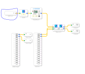
I've been using the "BEOCREATE 4 by B&O"( Beocreate_board_Link ) which uses a raspberry Pi as a controller interface for the DSP <> sigmastudio via network TCP, and can tweak settings in sigmastudio block modules (PEQ, compress.. volumes, etc) in real time before pushing/writing project to board. I'm hoping I can play with the settings the same way until reaching final config.
Thanks!
Are you able to control the modules in sigma in real time while connected with the USB?
I'm looking to buy the same set as yours.
I've been using the "BEOCREATE 4 by B&O"( Beocreate_board_Link ) which uses a raspberry Pi as a controller interface for the DSP <> sigmastudio via network TCP, and can tweak settings in sigmastudio block modules (PEQ, compress.. volumes, etc) in real time before pushing/writing project to board. I'm hoping I can play with the settings the same way until reaching final config.
Thanks!
@Tralalainan Yes, the modules can be adjusted and heard in real time if the project has had a "Link Compile Download". I managed to do a rough phase align for the woofer/tweeter using the delay module and a 2 channel scope and adjust the PEQ using pink noise. However, If a module is modified such as adding a band to a PEQ then the adjustments won't work until recompiled and downloaded. The feedback modules can also be used to read the rotary encoder and pot values, which I found useful for debugging.
That Beocreate board looks like an intriguing proposition considering the controllability via Pi, although I can't see any THD or output noise figures for the amp? Do you know which chip it uses? Not that I've researched, but If I could control the nvarcher board via Pi that would really complete my set up. I'm currently powering my DIY 2 way speakers through a pair of Aiyima TPA3250 boards with input from a QCC5125 BT decoder with reasonable (subjective but much better than Wondom JAB5) results.
That Beocreate board looks like an intriguing proposition considering the controllability via Pi, although I can't see any THD or output noise figures for the amp? Do you know which chip it uses? Not that I've researched, but If I could control the nvarcher board via Pi that would really complete my set up. I'm currently powering my DIY 2 way speakers through a pair of Aiyima TPA3250 boards with input from a QCC5125 BT decoder with reasonable (subjective but much better than Wondom JAB5) results.
@JimB91
The Beocreate is made by Bang & Olufsen so I would expect the best I suppose.
https://create.bang-olufsen.com/project/re-create
Great initiative from B&O.
I've tried their pi HiFiBerryOS but ended up with raspios and customising dsp via tcp sigmastudio.
I didn't think to use the pi to control the ADAU1452 you've got.
I'm now slightly concerned about the DACs on your board, how are they?
@Tralalainan
I'm quite new to DSP/DAC/ADC and don't have a great deal of exposure and points of reference but the CS42448 codec on the nvarcher ADAU1452 for me sounds superior to the Wondom ADAU1701 implementations I have. I've tried to match SNR figures in my set up to at least the same or better than the 108dB of the CS42448 but I'm only streaming 16bit audio so presumably that is the limiting factor? In terms of clipping I have found an input voltage greater than 1.4Vrms leads to distortion and therefore won't run the TPA3250 to full power, though it's still more than enough for my 30W drivers.
I'm no expert so please feel free to correct me if I'm wrong but maybe if the amp you use with the CS42448 has a less than 108dB SNR then it would be detrimental to the audio quality? I see now the Beocreate has TPA3128 chips with a 102dB SNR so maybe I'm hung up on SNR and THD+N figures and it's in the implementation? I must do some more research on the subject...
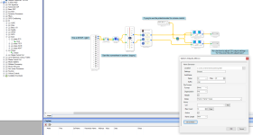
Hi all! After a bit of experimentation I have the cheap ADAU1452 board discussed here working with a CY7C68013A board flashed with freeUSBi. As in, I can compile & upload in SigmaStudio. I'm having quite a difficult time learning SigmaStudio though. For the moment, all I'd like to do is route the SPDIF input to one of the I2S outputs and have it working with a DAC (the one built into the MA12070, specifically). For this I'll have to set some I2S settings. Basically I'm struggling with two questions at this point:
- What is correct and what is incorrect about what I've done so far (see attached)?
- Where do I adjust output I2S settings such as left- vs. right-justified, etc.?
Attachments
Potentiometr signal should be adjusted by "14" using aritmetic shift block , see below. My advice is try to use readback block to see what is happening with signals in real time.

Thank you for these, frobek! Looking forward to tying it out once I'm back home on Thursday 🙂
The other thing I need to figure out is how to drive the /ENABLE and /MUTE pins from the DSP's GPIOs, especially to do everything in the correct order.
The other thing I need to figure out is how to drive the /ENABLE and /MUTE pins from the DSP's GPIOs, especially to do everything in the correct order.
I'm having quite a difficult time learning SigmaStudio though. For the moment, all I'd like to do is route the SPDIF input to one of the I2S outputs and have it working with a DAC (the one built into the MA12070, specifically). For this I'll have to set some I2S settings. Basically I'm struggling with two questions at this point:
A good quick start guide for programming the ADAU1452 is the EVAL-ADAU1452REVBZ User Guide below. A few notes:
- The SPDIF input always needs to be routed through an ASRC if going to the DSP for processing. The same goes for I2S inputs unless your I2S devices are slaves (they use the DSP’s master clock and have the same Fs frequency). So normally your SPDIF and I2S devices go through ASRC’s.
- The name of the Asrcin1 block confused me at first. It’s actually the ASRC’s outputs to the DSP core. From the DSP core’s view it’s an input.
- Setting the Fs frequency in the schematic only sets up the filters and other components to operate at that frequency. It’s your responsibility to set up the clock system so the correct Fs frequency is generated for the DSP core. You do this in the clock control tab in the register window. See the “Clock Generators” section in the ADAU1452 datasheet and Figure 18 in particular.
Attachments
Hi frobek, hi ernperkins,
so ... life happened and it was only yesterday evening I got a chance to play with this again.
See attached for what my sketch/program/circuit now looks like (what do people call these visual programs?)
This is after following your instructions as far as I understood them and reading over the datasheet's Clock Generator section.
Unfortunately, different from last time, something seems broken now: in the ADCIn1 widget, it's not possible anymore to select which input (according to the schematic, I would have to select ADC2 in order to get the potentiometer)
F7 output doesn't show any errors, the USB widget is green and "Write Latest Compilation through DSP" is working just fine, too. Completely stumped now 🙁
Attachments
Update: I was hitting https://ez.analog.com/dsp/sigmadsp/...he-knobs-or-sliders-in-my-sigmastudio-project ... after resetting the zoom level to normal, the UI works fine again.
Still no reading from the ADC, though. The readback is stuck at -5.9E-08.
Made triple-sure all blocks are set to 48 kHz.
Still no reading from the ADC, though. The readback is stuck at -5.9E-08.
Made triple-sure all blocks are set to 48 kHz.
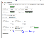
Check if your potentiometer is connected to the correct input, ie. AUX_ADC2 - ADAU1452 PIN10, see datasheet page 16/17.Still no reading from the ADC
Are you saying the schematic PDF published here may be inaccurate, frobek? I'll break out the multimeter and try to check best as I can (the pins on the IC are really small) but I'd be surprised if it was a hardware problem and not simply PEBKAC.
Schematic was posted 2-3 years ago, everything could happen during this time, but it was just a suggestion 🙂 . Readblock shows 0V which means that no voltage is connected to pin no. 10. But there is something wrong on your picture, AUX_ADC block should look like this:

on your schematic the block is "empty".
on your schematic the block is "empty".
Last edited:
- Home
- Source & Line
- Digital Line Level
- low cost ADAU1452 China board...