The TDA1543 output signal can be amplified using simple discrete amplifiers with a gain of 4, this can already be achieved using a single JFET
Do you have a schematic? e.g. with 2SK170?
EC,
Very interesting ideas & solutions - did you get to measure the output jitter from your master clock & at the I2S into the DAC? Can you publish these?
Did you use a DSP rather than FPGA for noise & clock distortion reasons? Within an FPGA you could have probably performed the SD card reader & I2S generation while allowing future-proofing! Is an FPGA much worse than a FPGA? What final uC will you be using? What is the minimum MIPS that it needs?
Hi -ecdesigns-
This is one of the most interesting projects around here; lots of good ideas and a really good concept. I'm not sure if you are designing this for an audio company; if so, please let us know in time when, from whom, and under which name it will be available.
Since SD-cards are quickly getting cheaper and also bigger and bigger in memory, I would advise to plan for somewhat higher capacity cards, like 32, 64 or even 128 GB, just to make the system future proof. Even 128 GB can still be easily formatted with FAT32, although it is advisable to use a relatively large cluster size. Since the individual track files are all quite large, there is no problem with wasted space. I'm assuming that your system can handle FAT32 with large cluster sizes. For the sake of simplicity, I wouldn't even support FAT16, which only has its place with small cards that may not be of interest any more at the time the player is on sale.
I think there would be a lot of interest to buy your player as a kit with an I2S output, and then combine it with a DAC of choice (presently the Buffalo 32S with the newest ESS Sabre chip should make a good match) into one housing.
I wish you luck and good progress with this project!
Kurt
Hi jkeny,
I haven't got suitable measuring equipment for measuring these low jitter levels. I attached an oscillogram of the produced sine wave signal of the simple 3-crystal version (11.2896 MHz / 5.5Vpp) at the input of the active element. Time division approx. 20ns / div. There is no visible jitter (very thin lines), at max. timebase setting (X10). The oscilloscope has a bandwidth of 60 MHz.
The actual output signal was shaped to have relatively fast positive going transients and relatively slow negative going transients in order to lower interference (square-wave with very fast transients creates a lot of unwanted side-bands).
The oscillator was designed for lowest possible frequency deviations at power supply voltage fluctuations between 5 and 8 volts (3V ripple).
The clock signal extraction and buffering circuit was designed to provide lowest possible frequency fluctuations at varying (capacitive) loads.
This resulted in a highly unusual design with up to 12 crystals.
We use a Microchip dsPIC 33FJ128GP02-I/SP (16 bit / 128K), it has all required hardware on-chip (clock multiplier, DMA, RAM buffers, DCI module), and provided lowest interference levels.
We run it at almost maximum speed of 40 MIPS (40 million instructions / second). Other advantage is the availability of Microchip FAT16/32 library, my brother has further optimized this library. We use the SD-card SPI interface (approx. 13 MHz clock frequency). This controller reads the SD-card, outputs I2S, scans the keys, receives RS232 commands (remote control) and sends RS232 commands (LED display). We read the SD-card DATA and directly put it in the RAM buffer (DMA transfer). The on-chip hardware (DCI-module) provides the I2S signals.
The LED display is scanned by a second PIC24FJ64GA002-I/SP (16 bit / 64K). It receives RS232 data from the dsPIC controller.
The display controller runs on the 11.2896 MHz master clock (single clock load), and an on-chip prescaler provides 5.6448 MHz clock for the dsPIC controller. The dsPIC controller has on-chip multiplier to achieve required clock frequency.
The second master clock output is used to drive a single (little logic series), fast D flip-flop (single clock load), that is used to synchronously reclock the 1.4112 MHz bit clock from the dsPIC controller.
did you get to measure the output jitter from your master clock & at the I2S into the DAC? Can you publish these?
I haven't got suitable measuring equipment for measuring these low jitter levels. I attached an oscillogram of the produced sine wave signal of the simple 3-crystal version (11.2896 MHz / 5.5Vpp) at the input of the active element. Time division approx. 20ns / div. There is no visible jitter (very thin lines), at max. timebase setting (X10). The oscilloscope has a bandwidth of 60 MHz.
The actual output signal was shaped to have relatively fast positive going transients and relatively slow negative going transients in order to lower interference (square-wave with very fast transients creates a lot of unwanted side-bands).
The oscillator was designed for lowest possible frequency deviations at power supply voltage fluctuations between 5 and 8 volts (3V ripple).
The clock signal extraction and buffering circuit was designed to provide lowest possible frequency fluctuations at varying (capacitive) loads.
This resulted in a highly unusual design with up to 12 crystals.
Did you use a DSP rather than FPGA for noise & clock distortion reasons? Within an FPGA you could have probably performed the SD card reader & I2S generation while allowing future-proofing! Is an FPGA much worse than a FPGA? What final uC will you be using? What is the minimum MIPS that it needs?
We use a Microchip dsPIC 33FJ128GP02-I/SP (16 bit / 128K), it has all required hardware on-chip (clock multiplier, DMA, RAM buffers, DCI module), and provided lowest interference levels.
We run it at almost maximum speed of 40 MIPS (40 million instructions / second). Other advantage is the availability of Microchip FAT16/32 library, my brother has further optimized this library. We use the SD-card SPI interface (approx. 13 MHz clock frequency). This controller reads the SD-card, outputs I2S, scans the keys, receives RS232 commands (remote control) and sends RS232 commands (LED display). We read the SD-card DATA and directly put it in the RAM buffer (DMA transfer). The on-chip hardware (DCI-module) provides the I2S signals.
The LED display is scanned by a second PIC24FJ64GA002-I/SP (16 bit / 64K). It receives RS232 data from the dsPIC controller.
The display controller runs on the 11.2896 MHz master clock (single clock load), and an on-chip prescaler provides 5.6448 MHz clock for the dsPIC controller. The dsPIC controller has on-chip multiplier to achieve required clock frequency.
The second master clock output is used to drive a single (little logic series), fast D flip-flop (single clock load), that is used to synchronously reclock the 1.4112 MHz bit clock from the dsPIC controller.
Attachments

I've been following this, very interesting. I believe this architecture is an excellent avenue to explore for hi res audio. All hard drive based systems I've heard so far have had plenty of digititus!
Can I also make a plea for I2S to be available for existing DACs to be used.
Keep up the good work and thanks for sharing EC
Can I also make a plea for I2S to be available for existing DACs to be used.
Keep up the good work and thanks for sharing EC
Hi Javin5
No we (my brother and I) are not developing this for an audio company. Main reason for this design was constructing a suitable digital audio source for high performance digital audio playback using 16/44.1 format. I first had the illusion that this could be achieved by using a stand-alone DAC with suitable (re) clocking strategy.
If there is any interest in this project, I could also provide a SD-player module with I2S & clock outputs only.
It's not practical to have so many CDs on one single SD-card, as the user interface has limitations. We don't want to complicate the user interface either, because this would conflict with the main design goal.
Seems 32Gb is about maximum right now:
http://www.engadget.com/2009/01/08/panasonic-hoping-to-launch-64gb-sdxc-card/
Like I said, we have to wait until, both SDXC cards, and SDXC specs are available.
Yes this could be done, but audio interface properties may have to be changed (DCI module configuration) in order to output required format.
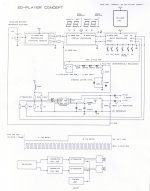
I attached a block diagram of the basic SD-card player. The master clock is a 3-crystal 11.2896 MHz version with 2 discrete clock buffers and an external battery reference voltage. This voltage is filtered and used for referencing the oscillator active element. One output drives the LED display controller, the prescaler on this controller feeds a 5.6448 MHz buffered clock to the main controller.
The display controller receives RS232 commands from the main controller to display required information.
The main controller reads the SD-card data and outputs I2S. It also scans the 6 keys that are used for CD, track selection, shuffle, start / pause and stop.
The 1.4112 MHz bit clock is then synchronously reclocked with a single high-speed D flip-flop (160 MHz ... 4 GHz), using the second master clock output. The clock signal is then fed to the DAC chip using a dynamic jitter attenuator circuit. It dynamically manipulates exact moment of triggering in order to achieve even lower sample timing jitter.
The other I2S signals (WS and DATA) are also attenuated in order to achieve lowest possible on-chip crosstalk.
The TDA1543 chip Vref pin is not connected (very important), an external reference voltage is used instead.
The timing diagram shows the I2S output signal.
The block diagram at the bottom shows how I connected the DAC, full output signal directly enters the power amp for achieving max. S/N ratio. The power distributed to the speakers is limited by a suitable attenuator. This greatly increases performance at lower volume settings that are most often used.
This is one of the most interesting projects around here; lots of good ideas and a really good concept. I'm not sure if you are designing this for an audio company; if so, please let us know in time when, from whom, and under which name it will be available.
No we (my brother and I) are not developing this for an audio company. Main reason for this design was constructing a suitable digital audio source for high performance digital audio playback using 16/44.1 format. I first had the illusion that this could be achieved by using a stand-alone DAC with suitable (re) clocking strategy.
If there is any interest in this project, I could also provide a SD-player module with I2S & clock outputs only.
Since SD-cards are quickly getting cheaper and also bigger and bigger in memory, I would advise to plan for somewhat higher capacity cards, like 32, 64 or even 128 GB
It's not practical to have so many CDs on one single SD-card, as the user interface has limitations. We don't want to complicate the user interface either, because this would conflict with the main design goal.
Seems 32Gb is about maximum right now:
http://www.engadget.com/2009/01/08/panasonic-hoping-to-launch-64gb-sdxc-card/
Like I said, we have to wait until, both SDXC cards, and SDXC specs are available.
I think there would be a lot of interest to buy your player as a kit with an I2S output, and then combine it with a DAC of choice (presently the Buffalo 32S with the newest ESS Sabre chip should make a good match) into one housing.
Yes this could be done, but audio interface properties may have to be changed (DCI module configuration) in order to output required format.
I attached a block diagram of the basic SD-card player. The master clock is a 3-crystal 11.2896 MHz version with 2 discrete clock buffers and an external battery reference voltage. This voltage is filtered and used for referencing the oscillator active element. One output drives the LED display controller, the prescaler on this controller feeds a 5.6448 MHz buffered clock to the main controller.
The display controller receives RS232 commands from the main controller to display required information.
The main controller reads the SD-card data and outputs I2S. It also scans the 6 keys that are used for CD, track selection, shuffle, start / pause and stop.
The 1.4112 MHz bit clock is then synchronously reclocked with a single high-speed D flip-flop (160 MHz ... 4 GHz), using the second master clock output. The clock signal is then fed to the DAC chip using a dynamic jitter attenuator circuit. It dynamically manipulates exact moment of triggering in order to achieve even lower sample timing jitter.
The other I2S signals (WS and DATA) are also attenuated in order to achieve lowest possible on-chip crosstalk.
The TDA1543 chip Vref pin is not connected (very important), an external reference voltage is used instead.
The timing diagram shows the I2S output signal.
The block diagram at the bottom shows how I connected the DAC, full output signal directly enters the power amp for achieving max. S/N ratio. The power distributed to the speakers is limited by a suitable attenuator. This greatly increases performance at lower volume settings that are most often used.
Attachments
To avoid misunderstanding as I am not sure I got the current flow right:
What is the voltage at pin 6 and 8?
What is the voltage at pin 6 and 8?
Hi EC,
I have a few basic questions about the SD player. Please illustrate me.
1) what is the function of the diodes in series with reclocked BCK? Don't they add noise?
2) is it OK to attach many I2S attenuators to one single choke? I guess BCK has to have it's own independent path...
3) doesn't the DC blocking cap form a too high HPF together with I/V R?
4) have you tried multiple series resistors (maybe SMD) on your DATA signal instead of one single 3K3?
Thanks in advance for the free lessons... 😀
Cheers,
M
revintage said:To avoid misunderstanding as I am not sure I got the current flow right:
What is the voltage at pin 6 and 8?
On my 1543 it measures 2.33V (with 3.1V battery).
John
Hi maxlorenz,
- Creating a suitable offset voltage of approx. 1.2V across 220nF. Without the diodes, the clock signal would partially discharge the 220nF cap, creating unwanted ripple voltage amplitude ( the diodes interrupt the bit clock signal below approx. 1.2V).
- The voltage drop across the Schottky diodes equals approx. 1.2V (3 x 0.4V). This is part of the requirement for correct bias level compensation.
- Schottky diodes produce almost no noise due to their specific properties.
- By placing 3 Schottky diodes in series, total capacitance is also reduced.
The circuit generates a DC bias voltage across 220nF, this voltage changes ever so slightly with bit clock duty cycle (jitter), thus changing the exact moment the TDA1543 triggers (and latches the outputs every 32 bit clock pulses). The time constant of the 220nF and 490R was tuned for lowest sample timing jitter and depends on application. The value of 499R depends on exact bit clock amplitude. The 220R series resistor is part of the attenuator that consists of 220 Ohm and 150 Ohm (the bit clock signal appears across the 150 Ohm resistor, 220nF is almost a short-circuit at these frequencies).
The effects of this circuit are similar to reducing master clock jitter amplitude. The circuit manipulates the exact moment the TDA1543 triggers (slightly earlier or later). This manipulation is done dynamically (duty cycle fluctuations result in bias voltage fluctuations), so it counter-acts jitter present on the bit clock (mainly the lower jitter frequency spectrum). This way the effects of the bit clock jitter can be compensated, leading to lower sample timing jitter (DAC output signal).
The choke is added to attenuate power supply noise. If you use multiple I2S attenuators (multiple DAC chips), it's best to use one choke for each chip.
BCK requires a separate circuit as crosstalk on this signal should be avoided.
This depends on connected load, I use a power amp with 47K input impedance (nothing else in between), with lower input impedances, the value of the coupling cap can be increased. I am still testing discrete buffer / amplifier circuits that may be included in the design.
I already tried this with previous designs like the DI4T, I still have to test what effect it has on this application. Multiple resistors in series increase inductance and reduce series capacitance. This may help to attenuate unwanted HF noise on I2S interface signals like WS and DATA.
The I2S signals also act as interference sources that usually flood the DAC chip with interference. That's why I use I2S attenuators / band limiters. These are dimensioned in a way that data integrity is maintained. By reducing I2S signal amplitude and reducing band width (causing less steep signal transients), on-chip ground-bounce at the I2S inputs can be greatly reduced. Now the DAC chip outputs less noise), and on-chip timing jitter level is reduced.
1) what is the function of the diodes in series with reclocked BCK? Don't they add noise?
- Creating a suitable offset voltage of approx. 1.2V across 220nF. Without the diodes, the clock signal would partially discharge the 220nF cap, creating unwanted ripple voltage amplitude ( the diodes interrupt the bit clock signal below approx. 1.2V).
- The voltage drop across the Schottky diodes equals approx. 1.2V (3 x 0.4V). This is part of the requirement for correct bias level compensation.
- Schottky diodes produce almost no noise due to their specific properties.
- By placing 3 Schottky diodes in series, total capacitance is also reduced.
The circuit generates a DC bias voltage across 220nF, this voltage changes ever so slightly with bit clock duty cycle (jitter), thus changing the exact moment the TDA1543 triggers (and latches the outputs every 32 bit clock pulses). The time constant of the 220nF and 490R was tuned for lowest sample timing jitter and depends on application. The value of 499R depends on exact bit clock amplitude. The 220R series resistor is part of the attenuator that consists of 220 Ohm and 150 Ohm (the bit clock signal appears across the 150 Ohm resistor, 220nF is almost a short-circuit at these frequencies).
The effects of this circuit are similar to reducing master clock jitter amplitude. The circuit manipulates the exact moment the TDA1543 triggers (slightly earlier or later). This manipulation is done dynamically (duty cycle fluctuations result in bias voltage fluctuations), so it counter-acts jitter present on the bit clock (mainly the lower jitter frequency spectrum). This way the effects of the bit clock jitter can be compensated, leading to lower sample timing jitter (DAC output signal).
2) is it OK to attach many I2S attenuators to one single choke? I guess BCK has to have it's own independent path...
The choke is added to attenuate power supply noise. If you use multiple I2S attenuators (multiple DAC chips), it's best to use one choke for each chip.
BCK requires a separate circuit as crosstalk on this signal should be avoided.
3) doesn't the DC blocking cap form a too high HPF together with I/V R?
This depends on connected load, I use a power amp with 47K input impedance (nothing else in between), with lower input impedances, the value of the coupling cap can be increased. I am still testing discrete buffer / amplifier circuits that may be included in the design.
4) have you tried multiple series resistors (maybe SMD) on your DATA signal instead of one single 3K3?
I already tried this with previous designs like the DI4T, I still have to test what effect it has on this application. Multiple resistors in series increase inductance and reduce series capacitance. This may help to attenuate unwanted HF noise on I2S interface signals like WS and DATA.
The I2S signals also act as interference sources that usually flood the DAC chip with interference. That's why I use I2S attenuators / band limiters. These are dimensioned in a way that data integrity is maintained. By reducing I2S signal amplitude and reducing band width (causing less steep signal transients), on-chip ground-bounce at the I2S inputs can be greatly reduced. Now the DAC chip outputs less noise), and on-chip timing jitter level is reduced.

Thanks EC for your detailed explanation (post#92).
I get the whole idea... 😀
Does the dynamic jitter attenuator perform better than your last BCK attenuator with RL to VCC?
Sorry, I meant one single choke for both, DATA and WS from the same chip...as per your diagram.
Maybe for multiple chips (DI4M) I can make a "quatrifilar" choke?
...and that invention improves significantly the sound of this humble chip 😉 to a level no one could imagine...
Cheers, Maestro .
M
The circuit generates a DC bias voltage across 220nF, this voltage changes ever so slightly with bit clock duty cycle (jitter), thus changing the exact moment the TDA1543 triggers (and latches the outputs every 32 bit clock pulses).
The circuit manipulates the exact moment the TDA1543 triggers (slightly earlier or later). This manipulation is done dynamically (duty cycle fluctuations result in bias voltage fluctuations), so it counter-acts jitter present on the bit clock (mainly the lower jitter frequency spectrum). This way the effects of the bit clock jitter can be compensated, leading to lower sample timing jitter (DAC output signal).
I get the whole idea... 😀
Does the dynamic jitter attenuator perform better than your last BCK attenuator with RL to VCC?
The choke is added to attenuate power supply noise. If you use multiple I2S attenuators (multiple DAC chips), it's best to use one choke for each chip.
Sorry, I meant one single choke for both, DATA and WS from the same chip...as per your diagram.
Maybe for multiple chips (DI4M) I can make a "quatrifilar" choke?
The I2S signals also act as interference sources that usually flood the DAC chip with interference. That's why I use I2S attenuators / band limiters. These are dimensioned in a way that data integrity is maintained. By reducing I2S signal amplitude and reducing band width (causing less steep signal transients), on-chip ground-bounce at the I2S inputs can be greatly reduced. Now the DAC chip outputs less noise), and on-chip timing jitter level is reduced.
...and that invention improves significantly the sound of this humble chip 😉 to a level no one could imagine...
Cheers, Maestro .
M
SD-player progress
Hi Tolu,
Not yet, but it's possible to merge WAV files into one continuous track if required. Perhaps the gapless playback function could be added later. Now a short drop-out (few milliseconds) is audible between tracks of a gapless album.
I plan to have it ready within a month.
The SD-player showed that sample timing jitter needs to be far lower than expected. I wasn't even able to achieve this using the 3-crystal ultra low jitter master clock and dynamic jitter reduction system (I need sample timing jitter of almost zero). Finally I apparently achieved this by tuning power supply decoupling, modifying discrete clock buffers, I2S attenuators, adding a dynamic noise feedback system between both DAC reference voltage and masterclock, and placing all critical circuits in copper boxes for optimal screening.
The result was so overwhelming that design was "frozen", and the SD-player has become my new reference. The sound quality resembles that what can be heard in recording studios and at live performances. The player also manages to reproduce dull recordings with exceptional clarity. Digital artifacts are no longer audible at all.
The same DAC circuit connected to a synchronously reclocked SPDIF or USB source performs badly by comparison, there is clearly audible distortion (digital artifacts), and dull recordings still remain sounding dull.
I am now working very hard to get the PCB design ready. The whole player basically fits on 3 PCBs:
- Front panel PCB with displays, drivers, and keys.
- SD-card holder PCB (for easy replacement)
- Main PCB woth processors, power supplies, 3-crystal master clock DAC and so on.
I plan to use no wiring, all connections are made through the PCBs, and the assembled module just slides into the housing.
I attached a sketch of how the SD-player is going to look like. On the front panel there is a display for CD selection (left) and track selection (right). The small orange LED in the center is on during playing and flashes during pause.
The two keys on the left are for disk selection (- / +) the two on the right are for track selection (- / +).
The right center key (with a small indication) is the play / pause button. the key right next to it is the stop key.
Pressing either CD or track selection keys increments / decrements disk or track selection and stops the player.
The decimal point on both disk and track displays indicate disk and / or track shuffle mode. Shuffle mode is entered by pressing the (-) key when the readout shows 01, the decimal point now comes on and stays on when increasing disk / track number, or toggles on / off when keep pressing the (-) key at 01.
The player is designed to keep playing continuously, sequentially playing all disks and than start over again. When disk and / or track shuffle is selected, the player continuously plays random disks and / or tracks.
The SD-card is entered in the center slot, label facing upwards. The SD-card holder is a push / push version, so pushing the SD-card after insertion ejects it again.
If no SD-card is inserted the display shows (-- --). If the inserted card contains no valid WAV files, the display shows (00 00).
On the rear panel there are the analogue outputs (L and R), remote power on/off (controls relay that switched power supply), and remote control (RS232 receive-only) RCA sockets. Power is applied using an external DC power source (mains adapter), this is better for safety reasons, and both mains interference and transformer magnetic fields are kept away from the SD-player electronics.
The housing is a standard anodized aluminum housing that comes in various colors (silver, gold, red, green, blue and black). The housing measures 1.77" (45mm) x 4.27" (108mm) x 8.66" (220mm).
Both front and rear panels are made from 2.5mm thick anodized aluminum. They are CNC milled and engraved. The display windows are CNC milled from colored transparent plexiglass.
I will also post some screen shots of PCB design progress soon.
Hi Tolu,
does your player support gapless playback?
Not yet, but it's possible to merge WAV files into one continuous track if required. Perhaps the gapless playback function could be added later. Now a short drop-out (few milliseconds) is audible between tracks of a gapless album.
When will it be available?
I plan to have it ready within a month.
The SD-player showed that sample timing jitter needs to be far lower than expected. I wasn't even able to achieve this using the 3-crystal ultra low jitter master clock and dynamic jitter reduction system (I need sample timing jitter of almost zero). Finally I apparently achieved this by tuning power supply decoupling, modifying discrete clock buffers, I2S attenuators, adding a dynamic noise feedback system between both DAC reference voltage and masterclock, and placing all critical circuits in copper boxes for optimal screening.
The result was so overwhelming that design was "frozen", and the SD-player has become my new reference. The sound quality resembles that what can be heard in recording studios and at live performances. The player also manages to reproduce dull recordings with exceptional clarity. Digital artifacts are no longer audible at all.
The same DAC circuit connected to a synchronously reclocked SPDIF or USB source performs badly by comparison, there is clearly audible distortion (digital artifacts), and dull recordings still remain sounding dull.
I am now working very hard to get the PCB design ready. The whole player basically fits on 3 PCBs:
- Front panel PCB with displays, drivers, and keys.
- SD-card holder PCB (for easy replacement)
- Main PCB woth processors, power supplies, 3-crystal master clock DAC and so on.
I plan to use no wiring, all connections are made through the PCBs, and the assembled module just slides into the housing.
I attached a sketch of how the SD-player is going to look like. On the front panel there is a display for CD selection (left) and track selection (right). The small orange LED in the center is on during playing and flashes during pause.
The two keys on the left are for disk selection (- / +) the two on the right are for track selection (- / +).
The right center key (with a small indication) is the play / pause button. the key right next to it is the stop key.
Pressing either CD or track selection keys increments / decrements disk or track selection and stops the player.
The decimal point on both disk and track displays indicate disk and / or track shuffle mode. Shuffle mode is entered by pressing the (-) key when the readout shows 01, the decimal point now comes on and stays on when increasing disk / track number, or toggles on / off when keep pressing the (-) key at 01.
The player is designed to keep playing continuously, sequentially playing all disks and than start over again. When disk and / or track shuffle is selected, the player continuously plays random disks and / or tracks.
The SD-card is entered in the center slot, label facing upwards. The SD-card holder is a push / push version, so pushing the SD-card after insertion ejects it again.
If no SD-card is inserted the display shows (-- --). If the inserted card contains no valid WAV files, the display shows (00 00).
On the rear panel there are the analogue outputs (L and R), remote power on/off (controls relay that switched power supply), and remote control (RS232 receive-only) RCA sockets. Power is applied using an external DC power source (mains adapter), this is better for safety reasons, and both mains interference and transformer magnetic fields are kept away from the SD-player electronics.
The housing is a standard anodized aluminum housing that comes in various colors (silver, gold, red, green, blue and black). The housing measures 1.77" (45mm) x 4.27" (108mm) x 8.66" (220mm).
Both front and rear panels are made from 2.5mm thick anodized aluminum. They are CNC milled and engraved. The display windows are CNC milled from colored transparent plexiglass.
I will also post some screen shots of PCB design progress soon.
Attachments

Will it be available as a kit (without enclosure) or if I interpret that sentence correct only as ready-built sales version.
Do you have any price ranges so far?
The result was so overwhelming that design was "frozen", and the SD-player has become my new reference. The sound quality resembles that what can be heard in recording studios and at live performances. The player also manages to reproduce dull recordings with exceptional clarity. Digital artifacts are no longer audible at all.
Do you have any price ranges so far?
Hi John.
It would be nice to think of an I2S output. This way you could attract a much wider community.
Not everybody might want to go for a new DAC at this stage.
Cheers
It would be nice to think of an I2S output. This way you could attract a much wider community.
Not everybody might want to go for a new DAC at this stage.
Cheers
Just wondering if it will be able to handle fragmented files?
I noticed that the ultimate source from koonlabs has a problem with them.
I'll be following this thread closely, because I'm very interested in this solid state player.
I noticed that the ultimate source from koonlabs has a problem with them.
I'll be following this thread closely, because I'm very interested in this solid state player.
Dear EC,
A month is not so long and the taxes cheque might arrive any time soon. I hope there will be a promotion price for faithful costumers
It is better to buy now before some big company buy/robs your idea...don't you think it is wise to apply for rights of the invention?
The little gap between tracks could be problematic for us, opera lovers, unless we copy on just one big tack: the entire Ring cycle on a single 8GB SD-card!!! 😎
I2S output is not such a good idea, I think, as it is said to deteriorate rapidly with a few inches length...that is why EC tried balanced I2S first, if I remember correctly.
About the enclosure, may I steal an expression from a dear forum mate? --> Fugly!
As I do not care a bit about the looks, it is the same for me...
Cheers,
M
- Status
- Not open for further replies.
- Home
- Source & Line
- Digital Source
- Lossless SD-card player