Hi EUVL,
I use 2SK117-BL and 2SJ103-BL, they are used in a unity gain complementary buffer.
May I ask what complementary JFET pair will work up to 12MHz ?
I use 2SK117-BL and 2SJ103-BL, they are used in a unity gain complementary buffer.
Hi rbroer,
I soldered them out of a Pentium II, 333MHz processor module.
Farnell has 1206 style 1uF/50V NPO
NTE ELECTRONICS|SMC1206Z105|Surface Mount Multilayer Capicators | Farnell Nederland
1uF NPO capacitors in 805 case style ???
Where did you find these, I want some.
I soldered them out of a Pentium II, 333MHz processor module.
Farnell has 1206 style 1uF/50V NPO
NTE ELECTRONICS|SMC1206Z105|Surface Mount Multilayer Capicators | Farnell Nederland
Hi rbroer,
I soldered them out of a Pentium II, 333MHz processor module.
Farnell has 1206 style 1uF/50V NPO
NTE ELECTRONICS|SMC1206Z105|Surface Mount Multilayer Capicators | Farnell Nederland
These are Y5V John. See its datasheet:
http://www.nteinc.com/capacitor_web/pdf/smc.pdf
I haven't seen NPO's much higher than a couple of nF's
The 2SK117 has 4 times the gain (transconductance) than the 2SJ103. Why didn't you use 2SK246 as complementary to 2SJ103 instead ?
And I hope your source resistance is substantially lower than 1k ?
Patrick
And I hope your source resistance is substantially lower than 1k ?
Patrick
EC
your new super clock looks very impressive.
How did you measure it ? Do you have any screenshots to show ?
Don't you worry that the square radiates back into the oszillator ?
your new super clock looks very impressive.
How did you measure it ? Do you have any screenshots to show ?
Don't you worry that the square radiates back into the oszillator ?
Hi EUVL,
I need 4 times the gain to get the circuit working as planned, the 2SK246 doesn't work in this circuit. 2SK117 also has lower noise.
Sources are connected directly together, and there is a 470 uH choke in the 2SJ103 drain, 2SK117 drain connects directly to +4V. DC bias current is set by JFET properties and requires no resistors.
The crystal oscillator output signal is also filtered by 4 crystals, this filtered output signal is used to drive the synchronous reclocker (most critical part). The oscillator buffered output is only used as "dirty" clock to drive the SD-transport. This doesn't mean it has high jitter, jitter on this output is still so low that I can't measure it with my test equipment.
The 2SK117 has 4 times the gain (transconductance) than the 2SJ103. Why didn't you use 2SK246 as complementary to 2SJ103 instead ?
I need 4 times the gain to get the circuit working as planned, the 2SK246 doesn't work in this circuit. 2SK117 also has lower noise.
And I hope your source resistance is substantially lower than 1k ?
Sources are connected directly together, and there is a 470 uH choke in the 2SJ103 drain, 2SK117 drain connects directly to +4V. DC bias current is set by JFET properties and requires no resistors.
The crystal oscillator output signal is also filtered by 4 crystals, this filtered output signal is used to drive the synchronous reclocker (most critical part). The oscillator buffered output is only used as "dirty" clock to drive the SD-transport. This doesn't mean it has high jitter, jitter on this output is still so low that I can't measure it with my test equipment.
Hi Bernhard,
Yes I performed the standard measurements as usual, but the capacity of the probe affects the measurements and the jitter level is too low to measure with my equipment.
So the real jitter "measurement" is done using selected CD recordings. After all, the reproduced sound quality is all that matters.
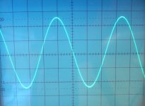
First oscillogram shows the sine wave output signal (that drives the capacitive node). It has already been filtered by 4 crystals that are also used for oscillation. I had to turn up beam intensity to get the camera focused. The flip-flop triggers on approx. 1V signal, the sine wave output (without probe connected) outputs approx. 12 ... 15Vpp with approx. 2.5pF load (trimmer plus capacitive node).
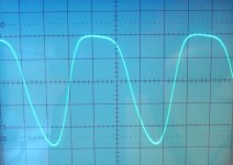
Second oscillogram shows the buffered output signal, this has slightly higher jitter as the signal has passed a discrete clock buffer, yet my equipment fails to show it. This output signal drives one clock load (processor).
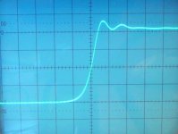
Third oscillogram shows the reclocked BCK signal in detail. This is the actual output signal from the on-board 180 Mhz synchronous reclocker.
The square wave runs in perfect sync with the crystal oscillator, I also took precautions to minimize crosstalk. Tests showed that the advantages of having a very short signal path between both oscillator and reclocker (few mm) outweigh possible crosstalk issues. This technique also allows to tap the crystal output signal without using buffers or comparators that do add some extra jitter.
your new super clock looks very impressive.
How did you measure it ? Do you have any screenshots to show ?
Yes I performed the standard measurements as usual, but the capacity of the probe affects the measurements and the jitter level is too low to measure with my equipment.
So the real jitter "measurement" is done using selected CD recordings. After all, the reproduced sound quality is all that matters.
First oscillogram shows the sine wave output signal (that drives the capacitive node). It has already been filtered by 4 crystals that are also used for oscillation. I had to turn up beam intensity to get the camera focused. The flip-flop triggers on approx. 1V signal, the sine wave output (without probe connected) outputs approx. 12 ... 15Vpp with approx. 2.5pF load (trimmer plus capacitive node).
Second oscillogram shows the buffered output signal, this has slightly higher jitter as the signal has passed a discrete clock buffer, yet my equipment fails to show it. This output signal drives one clock load (processor).
Third oscillogram shows the reclocked BCK signal in detail. This is the actual output signal from the on-board 180 Mhz synchronous reclocker.
Don't you worry that the square radiates back into the oszillator ?
The square wave runs in perfect sync with the crystal oscillator, I also took precautions to minimize crosstalk. Tests showed that the advantages of having a very short signal path between both oscillator and reclocker (few mm) outweigh possible crosstalk issues. This technique also allows to tap the crystal output signal without using buffers or comparators that do add some extra jitter.
Attachments
SD-transport project progress
Project progress,
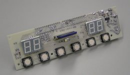
The new SD-transport module has been tested for some time now and works fine. I designed a separate SD-card holder module that requires no wires to connect to the SD-transport module. This ensures short connections and SD-card holder replacement (when contacts have worn out) within a minute. I attached a photograph of the SD-transport built on HF board and using the new SD-card holder module. The card holder module directly connects to the 7-way SD-card interface header.
This SD-transport requires 5V (white 4-way connector), 11.2896 MHz clock (2-way header), and an optional remote control signal (white 2-way header). It outputs I2S (5-way header), BCK (1.4112 Mhz), WS (44.1 KHz), and DATA. Signal levels are 3.3Vpp.
The two processors on top of the PCB are DSP and display controller. The 20 pin SMD chip is the segment buffer (74HC244). The 3.3mH panasonic choke is used for segment buffer power supply filtering. The SMD 3.3V regulator is an ultra low noise type from Micrel (specified @ 500nV). The design has been kept very basic, and standard components are used. Both processors are placed on IC sockets for easy replacement.
This SD-transport can drive all TDA154x chips and DAC chips with compatible I2S interface without any extra glue logic. The SD-transport accepts all SD/SDHC cards with speed rating of 2 or higher. Current support is up to 32Gb SD-cards, providing storage for over 50 Cds. Files are stored in WAV. Each Cd is placed in a separate directory. Every directory and track name has to start with a 2-digit number.
I plan to offer this SD-card module separately for diy, software for easy programming of SD-cards (works with iTunes) is for free. In order to provide compatibility with DAC chips that require 64 bits/frame (SD-transport outputs 32 bits/frame) I plan to design a small converter module.
We tested software that outputs 64 bits/frame on the current SD-transport, but then fast and expensive (speed rating 6) SD-cards are required. Processor noise levels and power consumption increase dramatically due to different data flow , and there is still some glue logic required to achieve correct I2S format.
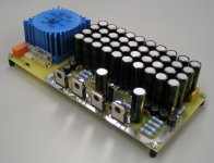
The DC-coupled high resolution bridge power amp modules are completed too. These will be used in the integrated SD-playback system. I attached a photograph of this single PCB bridge power amp. I designed two mirror-imaged versions for optimal placement in housing.
Most of the PCB area is occupied by the power supply. I used 40 smoothing caps, providing 2 x 30,000uF. The bridge rectifiers consist of fast, slow recovery diodes. The orange relay is used for power on/off through the system control module.
I also used some bulk metal foil resistors and a bulk metal foil trimmer for DC-offset adjustment. The power amp has balanced inputs and balanced outputs. All signal wiring will be hard wired (no connectors). Design is straight forward and optimized for high dynamic resolution.
The system control module and volume control / input selection PCB designs have been completed too. The system control module provides remote-control, volume control, input selection, muting, and power up/down functions.
Now there are 2 more modules to design, the dual 5V power supply and the first DAC module, based on a TDA1543. I also plan to design other DAC modules, including TDA1541A. I am also thinking of optional tube output stage modules.
Project progress,
The new SD-transport module has been tested for some time now and works fine. I designed a separate SD-card holder module that requires no wires to connect to the SD-transport module. This ensures short connections and SD-card holder replacement (when contacts have worn out) within a minute. I attached a photograph of the SD-transport built on HF board and using the new SD-card holder module. The card holder module directly connects to the 7-way SD-card interface header.
This SD-transport requires 5V (white 4-way connector), 11.2896 MHz clock (2-way header), and an optional remote control signal (white 2-way header). It outputs I2S (5-way header), BCK (1.4112 Mhz), WS (44.1 KHz), and DATA. Signal levels are 3.3Vpp.
The two processors on top of the PCB are DSP and display controller. The 20 pin SMD chip is the segment buffer (74HC244). The 3.3mH panasonic choke is used for segment buffer power supply filtering. The SMD 3.3V regulator is an ultra low noise type from Micrel (specified @ 500nV). The design has been kept very basic, and standard components are used. Both processors are placed on IC sockets for easy replacement.
This SD-transport can drive all TDA154x chips and DAC chips with compatible I2S interface without any extra glue logic. The SD-transport accepts all SD/SDHC cards with speed rating of 2 or higher. Current support is up to 32Gb SD-cards, providing storage for over 50 Cds. Files are stored in WAV. Each Cd is placed in a separate directory. Every directory and track name has to start with a 2-digit number.
I plan to offer this SD-card module separately for diy, software for easy programming of SD-cards (works with iTunes) is for free. In order to provide compatibility with DAC chips that require 64 bits/frame (SD-transport outputs 32 bits/frame) I plan to design a small converter module.
We tested software that outputs 64 bits/frame on the current SD-transport, but then fast and expensive (speed rating 6) SD-cards are required. Processor noise levels and power consumption increase dramatically due to different data flow , and there is still some glue logic required to achieve correct I2S format.
The DC-coupled high resolution bridge power amp modules are completed too. These will be used in the integrated SD-playback system. I attached a photograph of this single PCB bridge power amp. I designed two mirror-imaged versions for optimal placement in housing.
Most of the PCB area is occupied by the power supply. I used 40 smoothing caps, providing 2 x 30,000uF. The bridge rectifiers consist of fast, slow recovery diodes. The orange relay is used for power on/off through the system control module.
I also used some bulk metal foil resistors and a bulk metal foil trimmer for DC-offset adjustment. The power amp has balanced inputs and balanced outputs. All signal wiring will be hard wired (no connectors). Design is straight forward and optimized for high dynamic resolution.
The system control module and volume control / input selection PCB designs have been completed too. The system control module provides remote-control, volume control, input selection, muting, and power up/down functions.
Now there are 2 more modules to design, the dual 5V power supply and the first DAC module, based on a TDA1543. I also plan to design other DAC modules, including TDA1541A. I am also thinking of optional tube output stage modules.
Attachments
Hi maxlorenz,
I need complementary pairs (N-FET & P-FET), if I am correct, the power JFETs are only available as N-JFET. I am currently using 2 x 2SK1058 and 2 x 2SJ162 in the complementary H-bridge power buffer. Key factor however is power amp design.
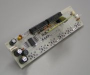
Meanwhile the second module of the Integrated SD-playback system has been completed and tested, its the new super clock / reclocker module. I added a photograph of this module. As you can see, a super clock doesn't need to be complicated.
The module contains 2 filtered LED shunt references (left). They provide both 4V power supply and 2V reference voltage. Decoupling was done using silvered mica caps, this was done based on both, measurements and listening tests. The complete module draws approx. 15mA @ 4V with one external clock load (SD-transport).
This super clock has 4 selected high-Q crystals (center). The crystals set oscillator frequency and perform oscillator output signal filtering. Fine-tuning is done with a Teflon trimmer.
Oscillation is maintained using a hybrid choke-loaded complementary JFET buffer. The gate resistor (100K bulk metal foil) connects to 2V reference voltage. The buffer produces both a 5Vpp square-wave and a 20Vpp sine wave output signal. These signal amplitudes are possible because of the hybrid chokes.
The 5Vpp square wave output signal is buffered by a matching hybrid choke-loaded complementary buffer and drives the SD-transport (1 clock load).
The 20Vpp low distortion filtered sine wave output drives a high-speed synchronous reclocker (located on the solder side) through a capacitive node. This capacitive node will have virtually no effect on crystal oscillator performance, it could be viewed as a wireless reclocker drive circuit. The reclocker is only a few millimeters away from the oscillator sine wave output, so it will perform way better than any external reclocker. The synchronous reclocker was preferred over a divider because a divider has more flip-flops and thus produces more jitter.
The synchronous reclocker has both, an external input and output. So one could reclock either BCK or WS.
The final design will be placed on HF PCB material (Teflon or comparable material). It also needs to be screened, I am thinking of a 2-layer screen consisting of copper and mu-metal.
In order to squeeze maximum performance out of this super clock, I used a 20th order LC power supply low-pass filter (10 x L, 10 x C) that also limits the current for the on-board shunt regs.
Hi Ecdesigns,
Ive been watching this forum for a while now and stumbled across this post about creating a low jitter clock. I was thinking about building one of these in the future and thought wouldn't it be cool if you could use a Xtal to act as a passive filter (no jitter) for another Xtal that is in active oscillation (jitter). Is this what you have done? Anyways your projects are awsome.
Dustin
merry x-mas
i wish you all, dear friends worldwide, a very merry x-mas and a happy new year with a lot of hifi high-end projects . 🙂
take care
mamal
i wish you all, dear friends worldwide, a very merry x-mas and a happy new year with a lot of hifi high-end projects . 🙂
take care
mamal

We use to wish all the best after the party 
 around here... but, anyway, I wish all my mates at the forum a better 2010, with lots of fulfilling experiences, especially to John who has given his time and effort to develop such nice units for us to better enjoy our music! 🙂
Cheers everybody!
M
around here... but, anyway, I wish all my mates at the forum a better 2010, with lots of fulfilling experiences, especially to John who has given his time and effort to develop such nice units for us to better enjoy our music! 🙂Cheers everybody!
M
Hi maxlorenz,
Thanks, I also wish everybody a better 2010.
ISD-playback system project is coming along fine. Two more modules to go for the basic version (DAC plus power supply module).
I spent weeks on the ISD-playback system power supply. Finally it will be a single 5.4V power supply feeding all circuits except for the two bridge power amps.
This power supply consists of two series cascaded, filtered LED referenced discrete regulators (9.4V regulator feeding a 5.4V regulator). The main advantage is greatly improved ripple rejection. It is very important to filter-out mains 50/60 Hz frequency plus harmonics. Single regulator is unable to achieve this.
The already very clean DC output voltage of this supply will be further filtered (20th order low-pass) for critical (reference) voltages. All integrated regulators that I was using before (78xx and comparable suspects) were removed, except for the ultra low noise 3.3V Micrel regulator in the SD-transport module. But I might even replace this one with a discrete regulator.
Based on extensive tests, integrated IC regulators like 78xx, LM3x7, TL431 I personally arrived to the conclusion that these are not suitable for powering audiophile equipment due to dynamic resolution issues (the way the voltage regulator inter-acts with dynamic load changes).
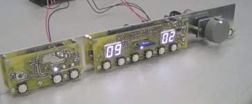
I attached a photograph of the front panel modules, mounted on an aluminum frame.
On the left is the new system control module. It provides IR remote control functions, power up/down, input selection (3 analogue inputs) and volume control (Motorized ALPS pot). The IR remote control now has 12 keys for controlling all required functions. The SD-transport is located in the center, and the volume control is on the right.
Keys (left to right) are for ON/OFF, input selection, disk-, disk+, stop, play/pause, track-, track+, and all the way too the right, muting.
Second picture shows how I plan to place the modules in the DI8-size housing.
High resolution DC-coupled bridge power amp modules are on the left and right. Most other modules are mounted on the front panel. The large space left is for power supply, DAC module (various DAC chip types possible), and optional DAC tube output stage plus power supply.
I wish all my mates at the forum a better 2010, with lots of fulfilling experiences, especially to John who has given his time and effort to develop such nice units for us to better enjoy our music!
Thanks, I also wish everybody a better 2010.
ISD-playback system project is coming along fine. Two more modules to go for the basic version (DAC plus power supply module).
I spent weeks on the ISD-playback system power supply. Finally it will be a single 5.4V power supply feeding all circuits except for the two bridge power amps.
This power supply consists of two series cascaded, filtered LED referenced discrete regulators (9.4V regulator feeding a 5.4V regulator). The main advantage is greatly improved ripple rejection. It is very important to filter-out mains 50/60 Hz frequency plus harmonics. Single regulator is unable to achieve this.
The already very clean DC output voltage of this supply will be further filtered (20th order low-pass) for critical (reference) voltages. All integrated regulators that I was using before (78xx and comparable suspects) were removed, except for the ultra low noise 3.3V Micrel regulator in the SD-transport module. But I might even replace this one with a discrete regulator.
Based on extensive tests, integrated IC regulators like 78xx, LM3x7, TL431 I personally arrived to the conclusion that these are not suitable for powering audiophile equipment due to dynamic resolution issues (the way the voltage regulator inter-acts with dynamic load changes).
I attached a photograph of the front panel modules, mounted on an aluminum frame.
On the left is the new system control module. It provides IR remote control functions, power up/down, input selection (3 analogue inputs) and volume control (Motorized ALPS pot). The IR remote control now has 12 keys for controlling all required functions. The SD-transport is located in the center, and the volume control is on the right.
Keys (left to right) are for ON/OFF, input selection, disk-, disk+, stop, play/pause, track-, track+, and all the way too the right, muting.
Second picture shows how I plan to place the modules in the DI8-size housing.
High resolution DC-coupled bridge power amp modules are on the left and right. Most other modules are mounted on the front panel. The large space left is for power supply, DAC module (various DAC chip types possible), and optional DAC tube output stage plus power supply.
Attachments
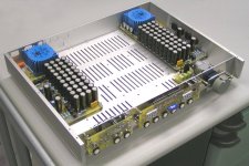
It looks wonderful! I can almost listen the crystal clear sound... 😀
I presume from the photo that you will install inner panels to divide the PS sections and heatsinking...
I expect to see the volume attenuator system soon...
You probably choose high quality connectors too...
Cheers,
M
I presume from the photo that you will install inner panels to divide the PS sections and heatsinking...
I expect to see the volume attenuator system soon...
You probably choose high quality connectors too...
Cheers,
M
Hi all!
I wish you also better 2010 and good health!
It seems my single box solution comes to reality! 😀😀😀
No fancy cables, connectors... even between innner modules they will be interlinks direcly soldered.
I like design also. It look very compact.
As you see from foto, for start it will be relays for input and motorised Alps potentiometer. It seems it satisfy high resolution sound.
Me also waiting for SD card player. I already bought some SDHCs.
Best from
Bostjan
Based on extensive tests, integrated IC regulators like 78xx, LM3x7, TL431 I personally arrived to the conclusion that these are not suitable for powering audiophile equipment due to dynamic resolution issues (the way the voltage regulator inter-acts with dynamic load changes).
That's good to hear. Power supply in digital is a major key to good sound. No conventional power supply we've seen can cut it. Even in the most expensive "high-end" equipment, power supply is a major limiting factor.
However, the evil factor in the power supply is not the regulator but the rectifier. Low voltage rectifier tubes can do miracles in digital (in combination with good chokes and good paper in oil capacitors). Problem is that these parts are very rare (and poisonous). Besides that and other impracticalities, it's a ridiculously expensive solution, not an option.
Problem is there are no alternatives for the diodes. Each solution based on diodes (or batteries) sounds "digital" in comparison, jitter restricts the sound in all major areas: less dynamic, less relaxed, less harmonic coherency (rich natural timbres), less resolution etc.
So if you can come up with a regulator that can handle diodes (or batteries!) you might have gold (usually batteries are noisy under digital load).
What's important to realize when designing audio that everything is a field, don't think in electrons, think in fields. Both information and energy are transferred by a field, not by the electrons! The field is between and around the conductors, the (dynamic) shapes of the fields determine the sound. That's why different parts, materials, layouts, etc. can sound so very different.
Fields are connected (jitter can not be isolated with a simple buffer). Layout/circuit board design in digital audio is critical, you need to shape/guide each field, with each connection, each part. One large ground plane is not always the best solution to create clean paths for fields.
What you listen to from your speakers is regulated mains power modulated by the source. Power supply and signal path are integrated and both essential.
The main problem with power supplies in audio in general is restricted dynamics (so restricted energy) and distorted harmonic coherency (non-linear behavior for different frequencies). That's why simple power supplies and simple regulators can sound more dynamic and more natural (harmonically correct), but less clean than more advanced ones. It's difficult to design a clean power supply that has an extremely linear behavior over the audio frequency range. Usually the more you put in the chain, the more harmonic distortions you create. It's very difficult to put something in that corrects it again. A very good system will loose it's magic when a mains filter is placed in the chain. How could it's power supplies now what is correct? For a large part designing audio is preserving the essential qualities (which are all to often lost, in "high-end").
To come back to digital audio, in an optimal design each part has a power supply best suited for it's task, but you can not fully isolate parts, often it sounds (partly) better to share the transformer and rectifiers, or in some cases even a regulator, but you'll also loose other qualities by sharing. These are difficult balances, becoming more obvious when you regard the total design as a composition of fields. The DAC chip needs to have a power supply which can prevent jitter and preserve audio qualities, not an easy job, but there are also simularities.
Btw. I had the pleasure to visit John a few months ago and I'm impressed by his work. He's one of the very few designers I know who actually tries everything for himself, listens for himself what sounds best, instead of copying what should be good according general opinions. So much of what is written or generally thought about audio does not correspond with what I hear. I don't have the patience or skills to design this way myself (I think few people have). But it's the only way to raise above the poor standard that's set by todays "high-end" audio.
I can hardly wait to get the SD-player, but it's good to see he's really pushing the boundaries, searching for the best.
Hi Void 🙂
Your previous post is excellent! Now I am imagining the fields vibrating with energy 😉.
The truth is that every single part, material, layout matters, but who has the time to investigate all the combinations? With a certain amount of experience most of us would stick to a certain combination that proved effective in the past or that is up to our skills...anyway, John's work is always keeping me interested and curious about new approaches, apart the free electronics lessons 😀 I steal...
Best regards,
M
PS: "it is amazing how good this humble DAC chip can be made to sound"
Your previous post is excellent! Now I am imagining the fields vibrating with energy 😉.
What's important to realize when designing audio that everything is a field, don't think in electrons, think in fields. Both information and energy are transferred by a field, not by the electrons! The field is between and around the conductors, the (dynamic) shapes of the fields determine the sound. That's why different parts, materials, layouts, etc. can sound so very different.
The truth is that every single part, material, layout matters, but who has the time to investigate all the combinations? With a certain amount of experience most of us would stick to a certain combination that proved effective in the past or that is up to our skills...anyway, John's work is always keeping me interested and curious about new approaches, apart the free electronics lessons 😀 I steal...
Best regards,
M
PS: "it is amazing how good this humble DAC chip can be made to sound"
Hi void,
Semiconductor rectifiers switch-on fast, causing peak surge currents as the connected smoothing cap starts charging instantly. Similar, during fast switch-off they could induce back-emf (inductive loads including smoothing cap self inductance). These in turn result in unwanted switching noise, note that a Schottky barrier rectifier would not prevent this either, as it switches-on fast too, and causes similar peak currents as with plain silicon rectifiers. During switch-off, back-emf can also be induced by using a Schottky diode. The Schottky diode does have advantages over plain silicon rectifiers (reverse recovery characteristics).
Tube rectifiers switch-on and off more gradually (controlled), causing lower surge currents. Call it dynamic compression as the tube rectifier limits peak charge current similar as with a clipping tube amp. So using tube rectifiers can have advantages.
The rectifier switching noise spectrum depends on, and is shaped by connected smoothing and decoupling caps. This is why each (electrolytic) cap causes different perceived sound quality, as it produces a different switching noise spectrum. The switching noise spectrum then inter-modulates with the signals processed by the connected circuits so the effects become audible.
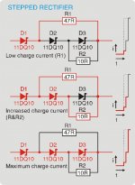
Now lets think "out of the box" for moment and observe attached schematics.
There are 3 Schottky diodes placed in series, each Schottky diode has approx. 0.4V threshold voltage (voltage across it needs to exceed this value in order for the diode to start conducting).
Upper circuit shows situation where V-primary just reached V-cap + 0.4V, only one diode (D1) can conduct now. The current has to flow though R1, so we start with a reduced charge current instead of full surge current that would occur with a plain rectifier (dotted line on the charge current graph).
As primary voltage rises to V-cap + 0.8V, D2 also switches-on and the charge current is further increased (D1, R1, D2, R2).
Finally, when the primary voltage exceeds V-cap + 1.2V, D1, D2, and D3 start conducting, bypassing R1 and R2. We have full charge current now.
Switching-off is also done step-wise in reverse order.
Resistor values need to be adapted to required load current.
What we achieved is a more controlled (step wise) switching of the rectifier and reduced surge currents (reduced switching noise). Number of diodes and resistors can be increased depending on allowable voltage drop and cost, for creating even lower switching noise levels. Simplest step rectifier would consist of 2 diodes and 1 resistor placed in parallel with one of these diodes.
I plan to use these stepped rectifiers in the ISD playback unit.
However, the evil factor in the power supply is not the regulator but the rectifier. Low voltage rectifier tubes can do miracles in digital (in combination with good chokes and good paper in oil capacitors). Problem is that these parts are very rare (and poisonous). Besides that and other impracticalities, it's a ridiculously expensive solution, not an option.
Semiconductor rectifiers switch-on fast, causing peak surge currents as the connected smoothing cap starts charging instantly. Similar, during fast switch-off they could induce back-emf (inductive loads including smoothing cap self inductance). These in turn result in unwanted switching noise, note that a Schottky barrier rectifier would not prevent this either, as it switches-on fast too, and causes similar peak currents as with plain silicon rectifiers. During switch-off, back-emf can also be induced by using a Schottky diode. The Schottky diode does have advantages over plain silicon rectifiers (reverse recovery characteristics).
Tube rectifiers switch-on and off more gradually (controlled), causing lower surge currents. Call it dynamic compression as the tube rectifier limits peak charge current similar as with a clipping tube amp. So using tube rectifiers can have advantages.
The rectifier switching noise spectrum depends on, and is shaped by connected smoothing and decoupling caps. This is why each (electrolytic) cap causes different perceived sound quality, as it produces a different switching noise spectrum. The switching noise spectrum then inter-modulates with the signals processed by the connected circuits so the effects become audible.
Now lets think "out of the box" for moment and observe attached schematics.
There are 3 Schottky diodes placed in series, each Schottky diode has approx. 0.4V threshold voltage (voltage across it needs to exceed this value in order for the diode to start conducting).
Upper circuit shows situation where V-primary just reached V-cap + 0.4V, only one diode (D1) can conduct now. The current has to flow though R1, so we start with a reduced charge current instead of full surge current that would occur with a plain rectifier (dotted line on the charge current graph).
As primary voltage rises to V-cap + 0.8V, D2 also switches-on and the charge current is further increased (D1, R1, D2, R2).
Finally, when the primary voltage exceeds V-cap + 1.2V, D1, D2, and D3 start conducting, bypassing R1 and R2. We have full charge current now.
Switching-off is also done step-wise in reverse order.
Resistor values need to be adapted to required load current.
What we achieved is a more controlled (step wise) switching of the rectifier and reduced surge currents (reduced switching noise). Number of diodes and resistors can be increased depending on allowable voltage drop and cost, for creating even lower switching noise levels. Simplest step rectifier would consist of 2 diodes and 1 resistor placed in parallel with one of these diodes.
I plan to use these stepped rectifiers in the ISD playback unit.
Attachments
Hi EC,
Would an RC (AKA snubber), tuned for the circuit, improve things over plain R?
R-C Snubbing for the Lab - Maxim
Would an RC (AKA snubber), tuned for the circuit, improve things over plain R?
R-C Snubbing for the Lab - Maxim
- Status
- Not open for further replies.
- Home
- Source & Line
- Digital Source
- Lossless SD-card player