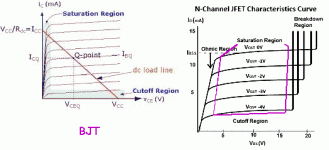
Shockley used the term saturation region for a JFET in 1953 this is in all major texts.
I have often been bothered by this.
A JFET is "saturated" when Vds is above say 5V-- where the curves flatten-out like a pentode. The middle of the curves.
In most BJT chatting we say "saturated" when Vce is *low*, tenths of a Volt. The left end of the curves.
These are not even the flip-side of the other, but very different concepts.
Attachments
I wouldn't get my hopes up.
There is an open source version of SUPREME.
I have often been bothered by this.
A JFET is "saturated" when Vds is above say 5V-- where the curves flatten-out like a pentode. The middle of the curves.
It's actually when the gate to drain pinches off and there is no abrupt knee like that graph it's a nice parabola to find the knee and a transition that (in the level 1 model) unfortunately has only the first derivative continuous. That graphic also loses the fact that JFET's have a triode region which can be put to use when one is pushed up against trying to get something to work on a single cell with 1V Vp FET's.
Last edited:
Scott, I am also a bit skeptical about the sales pitch. "Dear stranger, please figure out the fabrication details of the 2SC3503 discrete transistor which is no longer sold new, please put those details into SUPREME or another process simulator, and please run some simulations to show exactly what's going on in the so called quasi saturation region, then please post them here for us to all read. And please accept our grateful thanks in lieu of pay or barter."
simulations to show exactly what's going on in the so called quasi saturation region
I assumed they would do the work to prove their hypothesis.
....there is no abrupt knee like that graph... That graphic also loses the fact that JFET's have a triode region....
I will not argue the artistry of anonymous draftsmen found in a hasty Search. Yes, that JFET knee is ugly.
My point is: "saturation" in a JFET is "above the knee" and Shockley is our authority; OTOH "saturation" in a BJT (or pentode) is generally understood to be "below the knee".
I'm sure you know the difference. But I see less-experienced folks flummoxed by the different meanings.
And the ugly-knee JFET graphic shows an "Ohmic" area, your "triode region".
My point is: "saturation" in a JFET is "above the knee" and Shockley is our authority; OTOH "saturation" in a BJT (or pentode) is generally understood to be "below the knee".
The point being, I guess, is that there is ample tradition in the literature for the term "saturation" having some semantic flexibility.
And the ugly-knee JFET graphic shows an "Ohmic" area, your "triode region".
Except they drew it to imply only one resistance with no Vgs modulation
Last edited:
Very well said. I find transistor datasheets to be just about as useless as loudspeaker driver datasheets. A few specs are useful; max voltage, max current, max power. Those I believe. Everything else I measure.I'd have to dig around, but I would think that a good place to start looking would be for literature discussing how to extract SPICE parameters, where the authors will go through making the necessary measurements to determine the appropriate parameters.
I would not recommend the "SPICE models from the data sheet" type reviews out there as some of the parameters have to be evaluated from quite detailed behaviour which is not in the data sheet.
Some thoughts on the "Repi" theory of quasi -saturation:
measuring an MPSA42 gave a quasi-saturation resistance of about 250 ohms. Estimates (and these are very rough because I have no knowledge of the construction of an MPSA42) suggest that the epi layer is doped at about 1E15 (max, probably less) and the depletion region would extend to 20 microns at breakdown. If this were a 20 micron epi layer then the resistance works out about 25 ohms (but might be higher if the doping is less, or lower if my estimated area is too small). On the other hand, many of the older transistors were simply double diffused into a bulk substrate, without an epi layer. If this is 200 microns (this was a standard wafer thickness in days long past) then that resistance is about 250 ohms. Larger modern wafers may be thicker - hence depends on manufacturing again.
So again it is only through device simulation that the actual answer is to be found. That would show trends only without knowing precise constructional information.
Hi John,
If the depletion region extends to 20 microns at breakdown and the resistance would work out to about 25 ohms, then at low Vce (i.e., well below breakdown), where the depletion region is different, wouldn't the resistance work out to a different value?
Also, the 2SC3503 is likely a significantly bigger die than the MPSA42, suggesting that resistances may be lower.
I still think there is much more to it (quasi-saturation) than just voltage drop across the collector resistance. I think it is beta droop due to a combination of device physics issues going on, some of which are also involved in the Kirk effect.
Cheers,
Bob
Hi Bob
Yes, you may be right and the Repi theory wrong. So much for believing in text books.
Regarding the possible Kirk effect, simple calculations using basic principles suggest that it is more to do with Kirk than Repi.
A calculation of the epi resistance suggests that the carrier concentration is not so high as to cause what might be "limiting Kirk" effect where the carrier density is equal to the doping concentration. In this non-limiting case the carrier velocity is not saturated, and the calculations suggest quite a way below. Or, to put thie another way, the electric field across the epi is not very high to maintain the current (back to low resistances again).
However, in the depletion region the electric field will be higher and the velocity of carriers will be higher too. Whether they reach saturation velocity is another matter; it is often assumed they do but in a wider depletion region this might not be the case either.
In any case, this scenario suggests that as the carriers leave the depletion region and enter the epi, there is a transition region where they slow down. That could create a charge region, which, being negative (from electrons) would appear to be like the base, and extend the base width, in effect. That would reduce the gain of the transistor, hence reducing the current without incurring forward biassing of the junction.
If the carriers are velocity saturated in the depletion region there will almost certainly be a charge build up at the base side of the depletion region (rather than the collector end) and that will almost certainly widen the effective base width or at least add to the total base charge (Gummel number). Reducing the gain too.
Just some idle thoughts, may be wrong.
A device simulation would I am sure elucidate these points.
Last edited:
Well, two forward biased PN-junction diodes in one and the same transistor is an unholy scene, however, it can be shown that a huge Cob while dramatically increasing the Early effect, to the same degree minimizes the probability of the Kirk effect. A beautiful balancing act.
A high Cjc implies a higher doped epi layer which raises the current level at which the Kirk effect comes into play, as you say, but also reduces the epi resistance. OTOH a lower doping will raise the epi resistance and reduce the current level at which Kirk effect has an impact, which is more likely in high voltage transistors. Perhaps then, the "Repi" concept as an explanation for quasi-saturation came from this link. And that seems to have been picked up by compact modellers (SPICE type) rather than device physicists.
And that seems to have been picked up by compact modellers (SPICE type) rather than device physicists.
What makes you think these are different people?
I had the good fortune to work in Intel Process R&D in the early 80s, when Intel was kicking the rest of the world's ahsssz in high speed NMOS. Like, 40% faster than everyone else. Which pissed off the IBM guys to no end; remember, they had Robert Dennard, who "invented" (was the first to publish, cogently describe, and extrapolate) scaled MOS.
I can confirm that the device physicist who designed their transistors, was the same guy who created the SPICE** modeling equations and who extracted the numerical parameter values for those equations. Did he include the Frohman-Grove two parameter model of output conductance in the saturation region? (A. Grove being the President of Intel at the time?) Yes he did. Oh yes.
**Intel happened to use a different simulator called ASPEC at the time, probably for pre-historical reasons.
The Kirk effect refers to one of the BJT modes of operation (collector and emitter are nearly shorted, full conduction, small voltage over the device) that, just like the cutoff region (emitter-base junction is not forward biased, collector and emitter are open, small current over the device), is not used in audio amplifiers. The exploration of amplifying region should be of interest.
What is advantageous to inustrial applications, to which almost all approaches apply, may be found disadvantageous for audio. A strong neutral conceptual basis is needed to avoid being misguided.
When potential difference increases, electron density increases. As the collector-base capacitance increases, base width, input capacitance, current, transconductance are increased - impedance, magnetization and bandwidth are decreased. This is the Early effect. (I am more impressed by Miller`s insight published exactly hundred years ago, stating the same thing).
A small Cob is desirable for maintaining sufficient bandwidth thus, low distortion at high frequencies. Unfortunately, there are not any power transistors with small Cob.
The reverse recovery lifetime is much longer than the minority carrier lifetime, which is undesirable for transistors used as a switch. The minority carrier lifetime is intimately connected to voltage gain. In my notoriously controversial view, from a signal transfer point of view, a long transition time is preferable in both directions.
The genuine Sanyo 2SC3503 is a dedicated voltage amplifier. Considering the delicate nature of semiconductor fabrication, it would be of critical importance to avoid bogus manufacturers (easier said than done these days). The K(orean?)C3503 cannot possibly have anything to do with the original formula, it is just a common transistor made using simple technology and cheap tools.
The KSC3503 is the Fairchlid version, KEC does not make a 3503 variant IIRC. And there are measurements that suggest the Fairchild version has lower Rb than the NEC version.
What I look for in a transistor is the SOA (Safe Operating Area) which, looking at a curve tracer plot is between just turn on at bottom of curve up to just below the saturation roll off bend at top. This is the range of most linear response. It is also the slope you want to match in complimentary pairs.
Doc
Doc
The KSC3503 is the Fairchlid version, KEC does not make a 3503 variant IIRC. And there are measurements that suggest the Fairchild version has lower Rb than the NEC version.
KEC names are KTC3503 and KTA1381
Attachments
- Home
- Amplifiers
- Solid State
- Looking for a small signal NPN with no Quasi Saturation: MEASURED DATA