A cascode eats up a couple of volts keeping the high gain tranny biased. Quasi sat meany you just lose a couple of volts of undistorted voltage swing. Either way you lose a little output. Ok on 50 volt rails but maybe not on 10. You just need the right transistor - one that keeps all its beta at one or two volts. That’s why you were supposed to buy up a bunch of those C6043’s and the PNPs when they announced EOL.
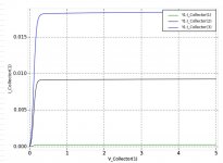
For the KSC3503E/KSA1381E circuit that I built and tested, it was a lot more than just a couple of volts. More like 10 volts and the problem was not just a loss of voltage swing.
As Bob stated, it depends on your application. If you have many gain stages and have the gain to spend on feedback, its not a big issue. For the simple circuits that I am exploring, the quasi-sat behavior dominates the large signal swing behavior of the circuit.
From N101N:
Wrong on all counts. As has been explicitly mentioned in at least two posts in this thread, quasi-saturation occurs when the base-collector junction becomes forward biased but externally the base-collector junction is still reverse biased. Due to the epitaxial collector resistance causing a voltage drop. And this resistance can be deduced from measurement.
Hard saturation occurs when the collector base junction externally is forward biased.
Velocity saturation is to do with how fast electrons can travel in silicon. Like terminal velocity of a body falling through the air.
Early voltage is another characteristic which can be measured. As James Early showed in his original paper.
I suggest you try reading about these effects.
Quasi saturation appears to be just a deceptive mathematical concoction not anchored in physical theory. You can`t measure saturation or the Early voltage neither experimentally nor mathematically,
Wrong on all counts. As has been explicitly mentioned in at least two posts in this thread, quasi-saturation occurs when the base-collector junction becomes forward biased but externally the base-collector junction is still reverse biased. Due to the epitaxial collector resistance causing a voltage drop. And this resistance can be deduced from measurement.
Hard saturation occurs when the collector base junction externally is forward biased.
Velocity saturation is to do with how fast electrons can travel in silicon. Like terminal velocity of a body falling through the air.
Early voltage is another characteristic which can be measured. As James Early showed in his original paper.
I suggest you try reading about these effects.
Last edited:
Even though saturation has a wide range of meanings in various areas of chemistry and physics, it is modelled comprehensively and consistently enough. The fuzzy expression quasi saturation is not found in authorative textbooks and can be safely removed from the vocabulary without losing descriptive power.
Saturation is used to describe the ever present restrictions on the motion of electric charge in both space and time due to stress, strain and a large difference between the properties of driving fields and the properties of conductive medium, increasing alarmingly with increasing charge density.
Saturation is used to describe the ever present restrictions on the motion of electric charge in both space and time due to stress, strain and a large difference between the properties of driving fields and the properties of conductive medium, increasing alarmingly with increasing charge density.
Even though saturation has a wide range of meanings in various areas of chemistry and physics, it is modelled comprehensively and consistently enough.
Shockley used the term saturation region for a JFET in 1953 this is in all major texts.
My criticism applies to the term Quasi Saturation. My impression is that saturation plays a prominent part in organic and biochemistry, but less so in physics and electronics.
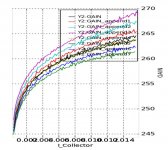
KSC2690AY
PB2 was kind enough to send me a few devices to run through the curve tracer.
The family of curves show that this transistor turn on quickly and turns on hard. No squooshy transition into saturation.
The gain curves are from Vce of 0.5V for the green curve at the bottom to Vce of 8V for the purple curve at the top.
Used in a VAS at 10mA, this transistor will have no more than 0.5 lost to gain compression at clipping.
You could also use this in a current source where you want minimum Vce.
Attachments
Star Shapes in Sub-Universe
The sub universe comment looks cryptic - no doubt those in the know will understand the message.
In your second bunch of tests the 2N2222 introduced by Motorola in June 1962 was advertised as having a star geometry and it has been described by some as the universal transistor.
According to the National Semiconductor Transistor Databook of 1982 that device is gold doped - being a non-overlay, double diffused silicon epitaxial device.
2N3904 from the same decade as 2N2222, and 2N2369 pages in that reference also refer to gold doping in their processes.
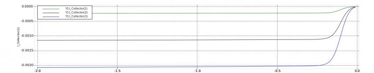
Thankfully the curve tracer plots attached to the first seven dozen posts in this thread, have given me some good ideas about which transistors to use and which to avoid, for good behavior during low Vce operation. If I studiously avoid the bad ones then I don't need to work out how to model quasi-saturation: in my little sub-universe of devices, it doesn't exist!
The sub universe comment looks cryptic - no doubt those in the know will understand the message.
In your second bunch of tests the 2N2222 introduced by Motorola in June 1962 was advertised as having a star geometry and it has been described by some as the universal transistor.
According to the National Semiconductor Transistor Databook of 1982 that device is gold doped - being a non-overlay, double diffused silicon epitaxial device.
2N3904 from the same decade as 2N2222, and 2N2369 pages in that reference also refer to gold doping in their processes.
If I recall, Gold doping was used to reduce carrier lifetime in transistors for when they went into saturation in digital applications. Not sure if it was used in non-saturating logic, like Shottky TTL. In any case, I was not under the impression that the 2N3904 was Gold doped.
Cheers,
Bob
"Process 21" is an overlay, double-diffused, gold doped, silicon epitaxial device. This device was designed for high speed saturated switching at collector currents of 10mA to 100mA. Principal device type: 2N2369
"Process 23" is an overlay, double-diffused, gold doped, silicon epitaxial device. This device is designed as a general purpose ampliier and switch. The useful dynamic range extends to 100 mA as a switch and to 100 MHz as an amplifier. Principal device type: 2N3904
"Process 23" is an overlay, double-diffused, gold doped, silicon epitaxial device. This device is designed as a general purpose ampliier and switch. The useful dynamic range extends to 100 mA as a switch and to 100 MHz as an amplifier. Principal device type: 2N3904
If I recall, Gold doping was used to reduce carrier lifetime in transistors for when they went into saturation in digital applications.
Cheers,
Bob
Thanks for that insight. Indeed there were a couple of processes in the databook for high speed logic and core driver applications that used gold doping.
From N101N:
Wrong on all counts. As has been explicitly mentioned in at least two posts in this thread, quasi-saturation occurs when the base-collector junction becomes forward biased but externally the base-collector junction is still reverse biased. Due to the epitaxial collector resistance causing a voltage drop. And this resistance can be deduced from measurement.
Hard saturation occurs when the collector base junction externally is forward biased.
Velocity saturation is to do with how fast electrons can travel in silicon. Like terminal velocity of a body falling through the air.
Early voltage is another characteristic which can be measured. As James Early showed in his original paper.
I suggest you try reading about these effects.
Hi John,
I've also seen the explanation in the literature that quasi saturation begins to occur when the "internal" base-collector junction is forward biased. In comparing that to ordinary saturation, where the "external" base-collector junction becomes forward biased, it is natural to conclude that the difference between the internal and external voltages where quasi-saturation and ordinary saturation occur is due to voltage drop in the collector resistance.
But I think that there is something wrong with that explanation because the voltage drop across the measured collector resistance cannot account for the higher voltage at which quasi saturation begins.
I measured the collector resistance of a 2SC3503 by forward-biasing the base-collector junction with the base and emitter connected together, making note of the current as a function of voltage drop. After taking proper account of the portion of the voltage drop due to the log portion of the Vbe, the ohmic portion of the base-collector voltage drop is divided by the current difference between two measurements. Doing this, the ohmic collector resistance of the 2SC3503 is less than 2 ohms. Even at 10 mA, the extra voltage drop due to collector resistance is only 20 mV.
In order for the collector resistance to account for the quasi saturation beginning to occur in the 2SC3503 at Vce on the order of 2-4V at collector currents in the range of 10-20 mA, the ohmic voltage drop in the collector resistance would have to be volts. Also, if quasi saturation was just saturation made to begin at a higher Vce due to ohmic voltage drop in the collector resistance, the quasi saturation characteristic would be much sharper.
I'm wondering if in the literature they are referring to something somewhat different than we think when they refer to the internal base-collector junction being forward biased at the onset of quasi-saturation. If so, such a description of the quasi saturation behavior would seem to be semantically confusing at the least.
Again, I think that quasi-saturation behavior is not so much related to ordinary saturation as we think of it (e.g., forward bias of the base-collector junction to the point where current flows that is a notable fraction of the base current) as it is to a falling off of current gain due to the physics of ordinary transistor behavior, as in things like base push-out, high injection and relative amounts of minority and majority carrier concentrations. I think it is largely just beta droop that occurs under conditions of low Vce and moderate collector current. This behavior will indeed be a function of collector doping concentration, but not really resulting from the increased collector resistance that typically accompanies a lightly-doped collector.
Cheers,
Bob
The behaviour in any semiconductor device is a complex interplay of diffusion, drift, rccombination and doping profiles. Carrier densities in the collector will affect the electric field profile, as will collector-base voltage, and electric field affects drift velocities, and the time carriers take to cross the collector will affect recombination and possible back-diffusion to the base.
Without knowing the doping profile its pretty much guesswork whats happening. If you know the profile its a routine modelling job to determine device characteristics as the basic physics of drift, diffusion, generation and recombination are very well known and readily simulated.
Without knowing the doping profile its pretty much guesswork whats happening. If you know the profile its a routine modelling job to determine device characteristics as the basic physics of drift, diffusion, generation and recombination are very well known and readily simulated.
Hi Bob
From the data sheet, the quasi-saturation resistance seems to be about 110 ohms, giving a 2V drop at about 18mA.
I'm not sure about your measurement at the moment, because a heavily forward biased diode will inject many carriers into the epi collector region, reducing its resistance through conductivity modulation that my first thought is that you are seeing the n+ substrate resistance. Particularly as the epi doping will be very light for a 300V transistor.
As you probably know there are several effects going on inside a transistor. High level injection effects occur at relatively low currents/bias voltages in lightly doped epi layers, leading to conductivity modulation, Kirk effect which would reduce the gain which could look like quasi saturation. Not all of these effects can be separated by measurement, but numerical simulation might reveal some useful insights.
Perhaps someone who knows the construction of some of these transistors and has access to a device physics simulator might investigate?
Yes, these are all good points and questions. From which curve on the data sheet are you inferring quasi-saturation resistance. 110 ohms seems awfully high if that is the collector resistance that has not been reduced by carrier injection from forward biasing of the base-collector junction. These complex effects that are mentioned by Mark are definitely over my head.
Cheers,
Bob
Cheers,
Bob
Mark got his response in while I was considering your post!
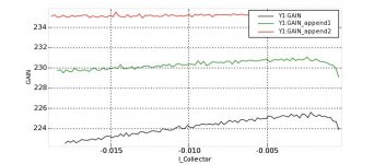
The datasheet graph of the static characteristics (fig. 1) shows a series of inflexion points which pretty much forms a line between the origin and 2V/18mA.
I agree that 110 ohms sounds high, but just as Mark pointed out, it is very difficult to deduce exactly what is going on without knowing the construction of the transistor. That means not only the doping profile but also the physical geometry.
If this is known, then as I implied and Mark stated, it is fairly straightforward to simulate these days.
It might be possible to deduce the collector epi resistivity from a CV measurement rather than high current injection. I'll think about that with an MPSA42 over the weekend.
Perhaps someone who knows the construction of some of these transistors and has access to a device physics simulator might investigate?
I wouldn't get my hopes up.
Mark got his response in while I was considering your post!
The datasheet graph of the static characteristics (fig. 1) shows a series of inflexion points which pretty much forms a line between the origin and 2V/18mA.
I agree that 110 ohms sounds high, but just as Mark pointed out, it is very difficult to deduce exactly what is going on without knowing the construction of the transistor. That means not only the doping profile but also the physical geometry.
If this is known, then as I implied and Mark stated, it is fairly straightforward to simulate these days.
It might be possible to deduce the collector epi resistivity from a CV measurement rather than high current injection. I'll think about that with an MPSA42 over the weekend.
Is there some publicly available writing concerning the CV measurements and how they correlate to the DC-IV behavior?
I think you're right Mark. Anyone with access to a device simulator is probably designing a new device. These transistors are pretty old and probably only the manufacturers know the construction in sufficient detail, and won't divulge.I wouldn't get my hopes up.
Is there some publicly available writing concerning the CV measurements and how they correlate to the DC-IV behavior?
I'd have to dig around, but I would think that a good place to start looking would be for literature discussing how to extract SPICE parameters, where the authors will go through making the necessary measurements to determine the appropriate parameters.
I would not recommend the "SPICE models from the data sheet" type reviews out there as some of the parameters have to be evaluated from quite detailed behaviour which is not in the data sheet.
- Home
- Amplifiers
- Solid State
- Looking for a small signal NPN with no Quasi Saturation: MEASURED DATA