Autumn's project is to stack DAC boards for higher output current - here are the prototype PCBs which just arrived. Only the baseboard (ground floor of the stack) needs the connection to the filter stage so that's arranged as a break-off part. Second and subsequent stories are then shorter boards.
This PCB is part of a 3 board DAC (assuming no stacking) - (1) DAC -> (2) filter -> (3) I/V & buffer. How many DAC boards can be successfully stacked is a matter for experiment. Beyond the idea of stacking to parallel more DACs comes the notion that other DAC chips can be experimented with and only board (1) needs to be substituted.
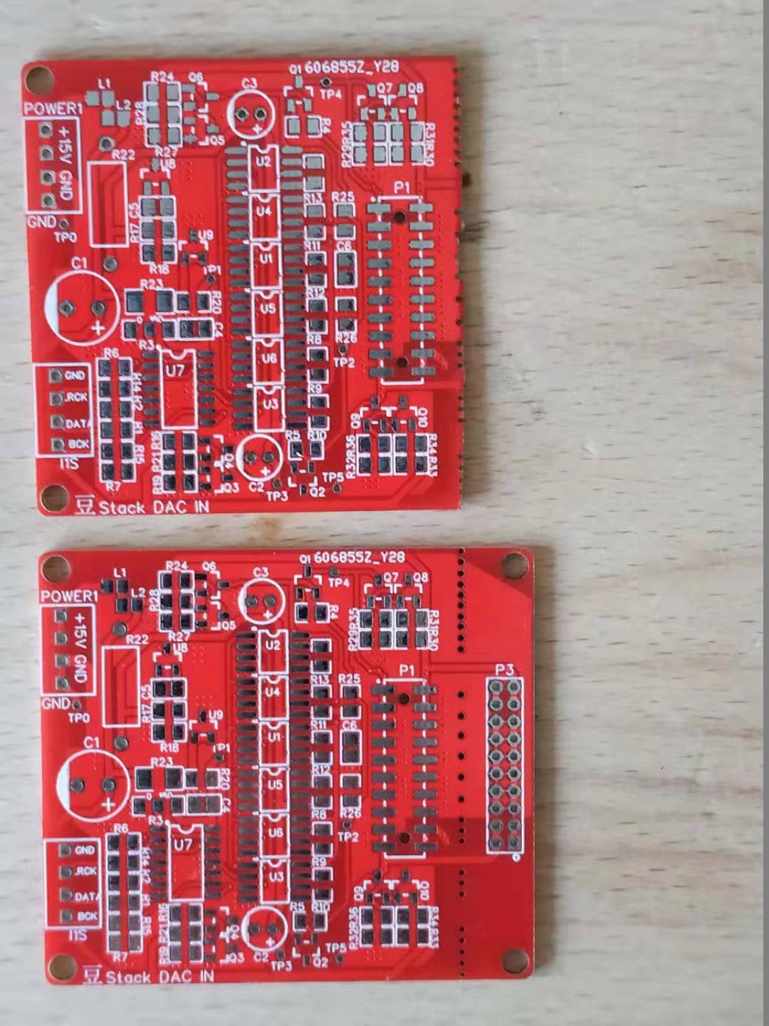
This PCB is part of a 3 board DAC (assuming no stacking) - (1) DAC -> (2) filter -> (3) I/V & buffer. How many DAC boards can be successfully stacked is a matter for experiment. Beyond the idea of stacking to parallel more DACs comes the notion that other DAC chips can be experimented with and only board (1) needs to be substituted.
Here's an experimental stack of 4 boards, in theory a total output current swing of 36mA into the I/V resistors. In the past when I've paralleled arrays of chips I've had problems with oscillation of the cascode MOSFETs - each block of chips has its own cascoding FET. For some reason they haven't liked being paralleled and have blown up randomly from parasitic oscillations. As I'm rather wary of that happening here I have arranged to test these 4 boards into passive I/V (330ohm) in mono balanced mode so the half-rail 7.5V zener doesn't get hit with the full DAC output current.
Since we only received 5 boards from JLC we're in need of more to see how high the stack can go....
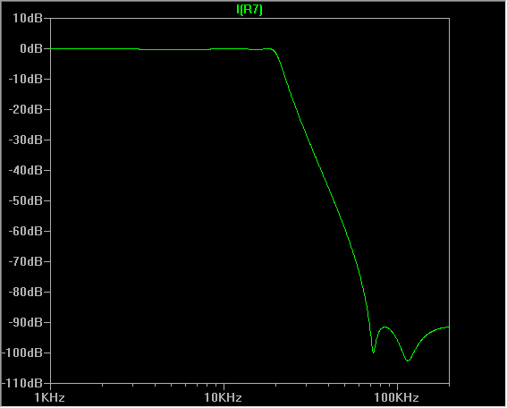
I've been working on a filter for 'Stack DAC' and I figured because I'm likely going to run it 2XOS that for a first pass, a 7th order will fit the bill.

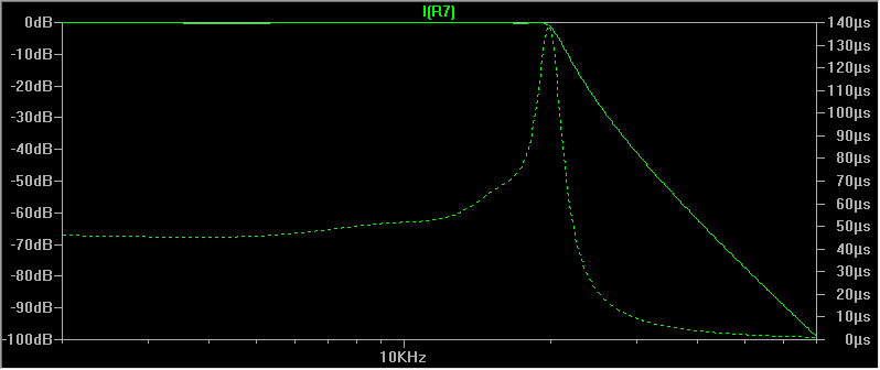
Passband flatness is around 0.2dB and at the band edge for 2XOS (68.2kHz) the attenuation is around -96dB so on target for a 16bit DAC.
With the I/V resistor of 270ohm a stack of 5 boards will give 4.3VRMS, double a normal CD player output.
Passband flatness is around 0.2dB and at the band edge for 2XOS (68.2kHz) the attenuation is around -96dB so on target for a 16bit DAC.
With the I/V resistor of 270ohm a stack of 5 boards will give 4.3VRMS, double a normal CD player output.
Here's the first gash prototype sequence of boards - 1) stack, 2) filter then 3) I/V-buffer stage. I haven't made a PCB yet for board 3 as I can't decide if I want an opamp or discrete one. The protoboard on the left holds the simplest possible buffer stage, just a CCS-loaded EF. The big electrolytic is needed to handle the transient high current demands on the mid-rail generator. It won't be needed when run balanced but I was keen to have a listen in stereo mode to what I've already built. And it sounds promising indeed.
For 5 boards and normal 2VRMS output level its also practical to have no buffer stage at all, just the I/V resistor which will be 125ohm.
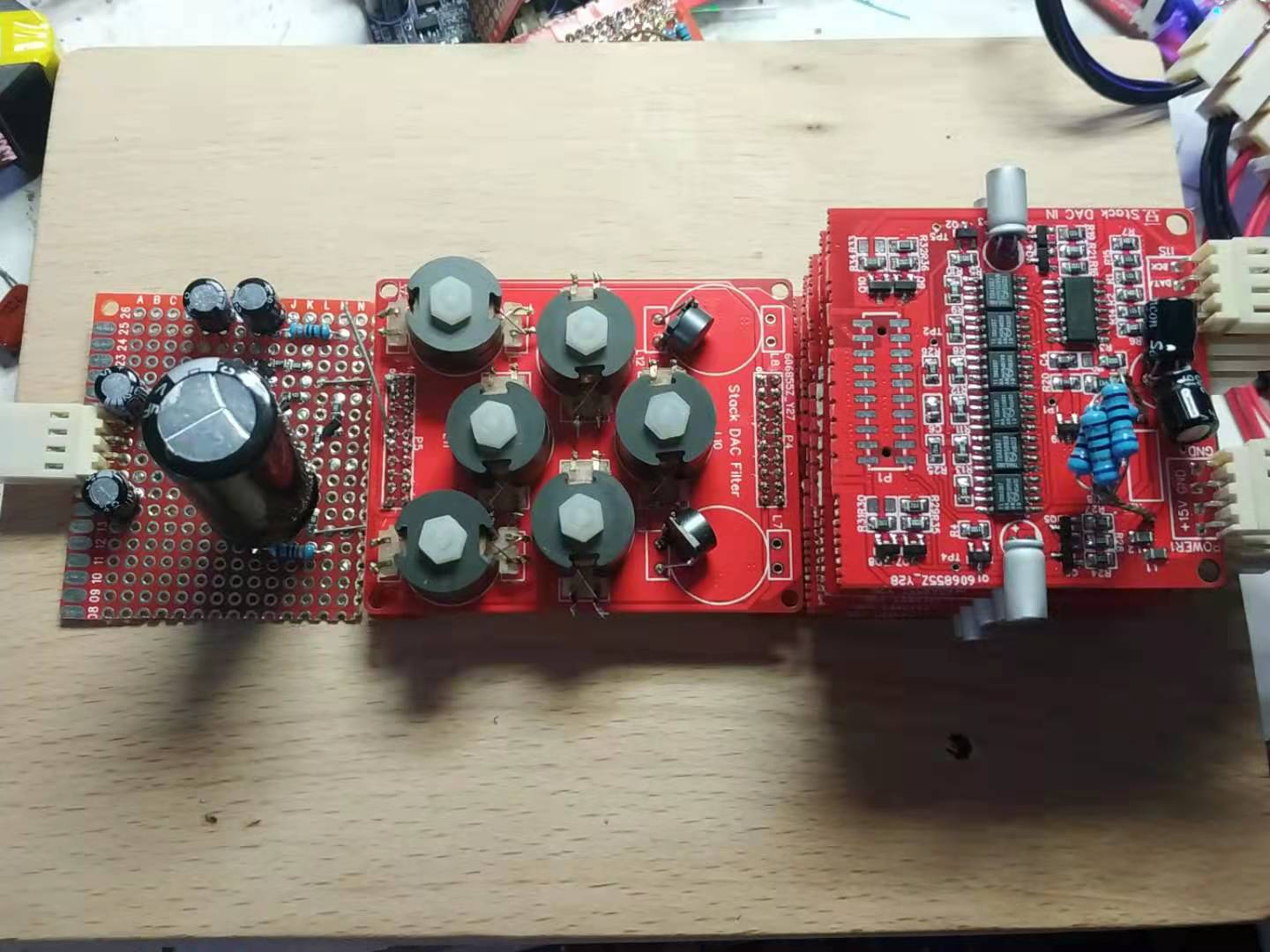
For 5 boards and normal 2VRMS output level its also practical to have no buffer stage at all, just the I/V resistor which will be 125ohm.
A couple of days of listening and its sounding really great, especially digging deep into the LF ambience on many recordings. I figure that's a direct result of lower noise through paralleling. But it runs so hot that it will never be a practical solution to box it up without a fan or other active cooling. So I'm going to need to modify it to run on two power rails rather than one as most of the heat is from the dropping resistors to power the DACs. The total power draw is 440mA at 15V so 6.6W. With an off-board PSU for the DACs I think I can halve that total. Or just double the number of chips for the same power.
There's a second generation stack PCB in the works thanks to wifey's dedicated layout work - this new one has 12 DAC chips per PCB so doubling the number of chips in the same height stack. But perhaps due to thermal constraints I need to think about arranging boards sideways rather than horizontally to encourage convection...
There's a second generation stack PCB in the works thanks to wifey's dedicated layout work - this new one has 12 DAC chips per PCB so doubling the number of chips in the same height stack. But perhaps due to thermal constraints I need to think about arranging boards sideways rather than horizontally to encourage convection...
Interesting idea Jim but its not the chips which are the major source of the heat, its the resistors feeding them. So I could mount the resistors on the Al substrate but I figure why not (effectively) move the resistors elsewhere (to the PSU, say) so that the DAC itself doesn't get too hot.
Oh of course yes sorry I overlooked that. A PSU less DAC would be interesting so we can try different flavours of PSUs . Not that there's anything wrong with your power designs you understand!
I don't like the idea of the PSU not being local for reasons of keeping current loops small to keep noise under control. So I'm unlikely to completely dispense with the PSU for the DAC chips, much as I like to accommodate customer wishes. I had the idea to pre-regulate the DAC PSU then use a shunt reg from a much lower input voltage (say 6.5V or 7V), that way the series element of the shunt isn't going to get so warm.
The shunt I'm using currently (TL431) isn't particularly quiet but I do expect some noise cancellation because each strip of 6 chips is fed with an independent shunt so any noise will tend to cancel to a degree (3dB) when those independent noise sources are added together.
@jimk04 I just had a thought - on the new 12-chip board you'll be able to bypass the DAC power supply completely and run your own power source direct to the chips. You just need to omit the TL431 shunts and fit 0R resistors as the series elements.
Last edited:
The next 5 boards for the 'hot' version turned up and I've employed them as a balanced channel, so now the DAC's got 10 boards, 5 for each channel and runs balanced. Adding more chips gives me the impression that the tonal density has improved. What I mean by 'tonal density' is (to use a video metaphor) that the saturation of timbral colours has increased a bit, all sounds are a little more rich somehow.
The 12 chip boards have also come in and I'm building up a couple to check out the heating factor.
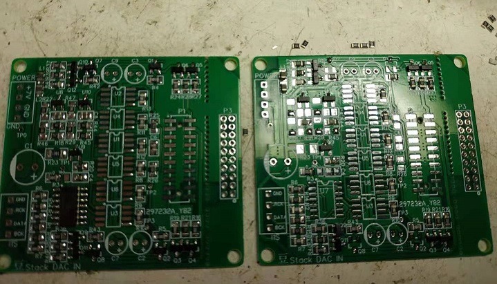
The 12 chip boards have also come in and I'm building up a couple to check out the heating factor.
From some fiddling around with filters in simulation, its possible to get close to 16bit stop-band rejection with a 5th order filter with some paralleled capacitors to create what are called 'stop-band zeroes'. Including the zeroes gives more attenuation at lower frequencies in exchange for worsening rejection higher up. But we need it less as the frequencies go up so that seems like a fair trade in this instance. Here is an example which I designed around the inductors, rather than designing from mathematical templates. Seeing as getting fairly close tolerance inductors off the shelf is rather tricky, here I'm using 3 pre-selected values in series to hit the target values (2.52mH and 2.11mH). We shall have to see how well this works out in practice with the inductor values that come off the reel. Going down to 5th order is what gives the opportunity to use lower Q inductors, in this case TDK SLF7045Ts.

Hi @abraxalito could You spot the diference in
Thanks 🙂
.
Could You post the phase of the filter please?
- passive filter prior Riv conversion, when the DAC Iout coupled to the reactive circuit
- and filter after the IV conversion when dac is not loaded with reactive elements.
Thanks 🙂
.
Could You post the phase of the filter please?
Yes. that is from vital importanceI don't like the idea of the PSU not being local for reasons of keeping current loops small
Hi @abraxalito could You spot the diference in
- passive filter prior Riv conversion, when the DAC Iout coupled to the reactive circuit
- and filter after the IV conversion when dac is not loaded with reactive elements.
I'm not confident I totally understand your question. But seems you might be asking about the difference between doing I/V conversion before vs after the LC filter. In the first case, having a passive filter prior to I/V conversion you need a DAC with a substantial output compliance, the filter's ringing exacerbates that at the top end of the frequency band. Most of the traditional R2R DACs don't have wide compliance, they're designed for virtual GND operation, TDA1387 and TDA1543 though do. I don't know of any others. Whereas my older designs went this route, nowadays I slip in a small signal MOSFET prior to the filter to improve the compliance even beyond what the TDA1387 has (0->3.5V typically). The reason for that is to optimize the SNR - the higher the value of the I/V resistor, the better so its best to go direct to 2VRMS (assuming that's the DAC's output level) rather than include a later gain stage which only adds noise.
With the I/V conversion done prior to the filter you'll typically have an I/V resistor doing the conversion, this R then defines the input impedance to the filter and you have a scheme which doesn't make as good use of the DAC output current as the first arrangement. Typically you'll have an LC filter with equal input and output impedances and this loses 6dB of signal. That's a significant hit to the SNR so I avoid that. Of course you could go active I/V prior to the filter but then the active element has to deal with a very wideband signal and that's generally going to make IMD.
Did I answer your question without fully understanding it?
Could You post the phase of the filter please?
The phase is shown with the dotted line, right scale. There's 360 degree of phase by 24kHz.
Thanks for the informations 🙂
.
I think that is simulated phase response?
Maybe do You have measured phase?
.
Thanks
Cheers.
.
I think that is simulated phase response?
Maybe do You have measured phase?
.
Thanks
Cheers.
Modified balanced stack running from two power rails (7.5V and 15V) to move the heat from the DAC boards to the offboard regs.
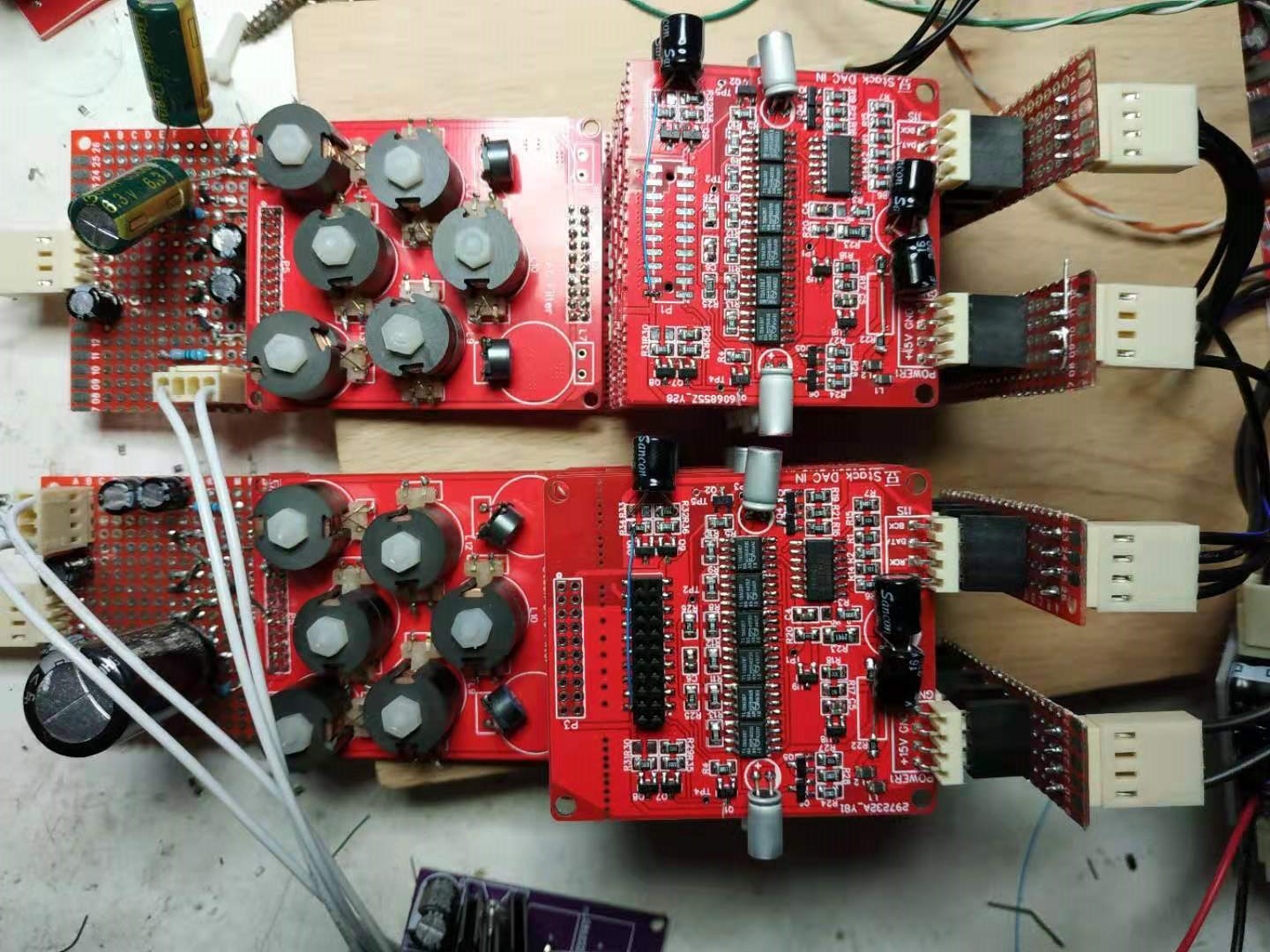
Rather than run separate cables (I2S and power) to each board I've created 'backplanes' so only one cable each for power, and I2S is required. Total current draw now 800mA at 17V. DAC boards only gently warm now, should be no issue boxing them up.
Rather than run separate cables (I2S and power) to each board I've created 'backplanes' so only one cable each for power, and I2S is required. Total current draw now 800mA at 17V. DAC boards only gently warm now, should be no issue boxing them up.
- Home
- Source & Line
- Digital Line Level
- lingDAC - cost effective RBCD multibit DAC design