Tekko you are a real ringing master 😀😀😀
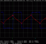
That's how my lower side gate waveforms look like at 5V/div (blue). Output inductor current waveform is also shown at 2.5A/div (red). I actually grounded the gate probe to the output of the amplifier and enabled AC mode, so there is some slight inaccurancy (my oscilloscope does not have floating inputs).
That's how my lower side gate waveforms look like at 5V/div (blue). Output inductor current waveform is also shown at 2.5A/div (red). I actually grounded the gate probe to the output of the amplifier and enabled AC mode, so there is some slight inaccurancy (my oscilloscope does not have floating inputs).
Attachments
I don't expect any iron powder core with a diameter equal or below 50mm to store more than 10mJ, or should I?
I think so. It depends on how much degradation is allowed in inductance. If it can be 30 %, then it's OK. For example this: Arnold Magnetics A-438281-2 shoud be able to store at least 50 mJ. Maybe this is not the best solution, but possiple.
How much heat produced by wire now?
Where can I send e-mail to?
Hey Tekko,
I never built your circuit, there was no fire, and all my breadboards still have their dust on them 🙂
I kind of wanted you to think a little bit and try it out before going and ordering another PCB that someone else made for you.
Did it work?
Cheers,
Chris
PS: Nice gate wave Eva.
I never built your circuit, there was no fire, and all my breadboards still have their dust on them 🙂
I kind of wanted you to think a little bit and try it out before going and ordering another PCB that someone else made for you.
Did it work?
Cheers,
Chris
PS: Nice gate wave Eva.
0.71mm diameter magnet wire gets too hot to be touched with just the +/-2.5A idle ripple current.
It wórked until i hooked up a 2x24v trafo, then it smoked, tho i think it was the boot diode that was the original cause.
Tho i am too frightened to try 2x38v again.
On 2x19 v it happlily plays bass up to rail/rail with no heat at all.
Tho i am too frightened to try 2x38v again.
On 2x19 v it happlily plays bass up to rail/rail with no heat at all.
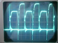
Tekko your waveforms always show problems such as strong gate drive ringing, asymmetric dead times, asymmetric duty cycle when idle and the like. You won't achieve reliable operation at high voltages until you solve each of these problems. Particularly, gate drive must be clean and dead time must be well defined and symmetrical before daring to try higher voltage rails.
Consider my prototype for example. Any cross-conduction or false turning on with 340V supply rails would destroy the IGBTs almost inmediately.
Consider my prototype for example. Any cross-conduction or false turning on with 340V supply rails would destroy the IGBTs almost inmediately.
Eva, if i adjust so gate waveforms are 50/50 i get over a volt on the output.
Why the waveforms have diff amplitude is because high ouput has higher voltages than the low output.
Why the waveforms have diff amplitude is because high ouput has higher voltages than the low output.
Hi!
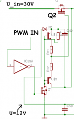
Does anyone has any ideas why the Q1 keeps blowing, when I apply some load to this circuit? It's a buck converter, not a Class-D amp, but the high-side driving is the same 🙂
The Q1 is a BSS123 MOSFET (Vdss=100V, Id=170mA, P-ch), thoose bipolar transistors are BCX 53/56 (i will post image from the mosfet's gate), and the Q2 FET is an FDP3632.
When the circuit is in idle, everithing is OK. When I apply a relative small load (the output current is about 10% of the nominal output current), then still it's OK. But when I load the circuit with a bigger resistor, to make approx. 10A, the BSS123 blows.
I tried soldering paralell the Q1 a bigger diode, becouse I saw some undershot on Q1's drain-source, but nothing improved, the Q1 blown.
I'm gonna try a diode between the U$3's base, and Q1's drain, maybe that will help.
What do you think if that?
Attachments
Workhorse said:
Hi Toino,
Dont you see that the Schottky is protected from reverse potential by the Antiparallel HEXFRED diode with Vf=0.6V
Cheers,
K a n w a r
Hi Workhorse
Maybe... but the HEXFRED is much slower than the Schottky…
Could you teach a little more, please?
Oops, sorry...
That's an N-ch FET, as the schematic shows, I just "misspelled"...
Do you have any idea, what can cause that FET's death?
That's an N-ch FET, as the schematic shows, I just "misspelled"...
Do you have any idea, what can cause that FET's death?
Eva, fredos, classd4sure, danko. What would be a good diode to put in parallel with the fets to protect from over/undershoot ?
RGP10G seem alittle slow, 1N4148 seem alittle weak on the current side.
RGP10G seem alittle slow, 1N4148 seem alittle weak on the current side.
Danko,
When Q1 turns on, U3s collector base junction can become forward biased while the MOSFET is still conducting. The current through this junction and Q1 needs to be limited.
Rick
When Q1 turns on, U3s collector base junction can become forward biased while the MOSFET is still conducting. The current through this junction and Q1 needs to be limited.
Rick
Eva said:High side MOSFET source is not at ground potential, it's floating as it's connected to the switching node!
ok 🙂
kartino said:Hi RX5,
Some people made the DIY UcD as well done. If you copy exaclty to real circuit then it shall work.
The high side as Eva said referenced to floating point. The low side referenced to negative rails. The audio referenced to each other between inverted and non inverted input. You can connect the ono inverted input to ground if your tone control referenced to ground.
regards,
kartino
ok.. 🙂
i have printed the schematic... im "studying" it now...
in th e miniUcD, (Q46,Q48) , (Q47,Q45).. wired like an SCR?? back to back transistors. ..what is this configuration called?? is it wired like a comparator <1 input from audio and another from the output<to maintain osc>?? so this is self oscilating.. and thos 4 transistors are referenced to the negative rail...
sorry for SO MANY QUESTIONS: just trying to learn here
i wonder if i could simulate it in workbench pro.. till then, ill post what I understand...

Danko, contrary to what the esteemed Kartino has said, I think you ought to play with that on the simulator awhile before making a go of it, for if you run into any problems, you stand a single chance at fixing it. Kartino has put some time in a simulator before making it happen as well. Myself, have put more in than I care to mention.
Pick up LTspice and simulate it with that!
Danko, I would do some research before recommending a Zener from gate to source, such a thing can easily be counter productive, and damaging, especially in a less than ideal layout, and when not applied properly.
Tekko, you can try solving that with improved layout, if you did it on a breadboard I would concentrate on other matters for the time being. There are excellent application notes on that topic, ask google my friend.
Cheers,
Chris
classd4sure: I was "playing" with simulator. I used "TINA". I don't know, if you know this program.
I have simulated only in DC mode, but it seems I have to simulate in AC.
Earlier /many months/ this type of high-side driving was working, but then I was using synchronous rectification, and I used dead-time. Maybe this is, why I haven't realized this mistake in this solution.
Thanks for "enlightening", classd4sure 🙂
Thanks the advice, sawreyrw!
- Status
- Not open for further replies.
- Home
- Amplifiers
- Class D
- level shifters and mosfet drivers