TOINO said:
Hi Tekko
Do you recognise this one?
Please note the group position of 3x100nF capacitors and the way they are connected to the Drain mosfets for decoupling…
Looking around, is easy to found some good Pcb routing examples at this power level.
I would be interested, how are the MOSFETs driven? I see only 2 ICs on the PCB, and they are too far from the MOSFETs. I don't think they are the mosfet drivers.
Re: Re: Re: chris, need info about your miniUcD
Hi,
Yes I recognize it.
This one you're looking at is one of the first I'd built and it had a few problems, you're going to have a hard time if you try using it.
You'll gain understanding of it by reading the patent and the reference design thread, along with transient simulation. This version is basically the patented version, with a little extra. You really ought to be able to answer each of the questions you asked yourself. The above reading will greatly help you do so.
This includes the bare minimal support circuitry required to allow it to work, and is a workable circuit both in simulation and in practice... It's the noobs dream! The practical values will change however, and you'll have to become familiar with it enough by your own research to enable you to tune it into a working amplifier. I actually expect that much.
Just remember if it seems like too much of a task, 99% of the work was already done for you, so I'll be pretty quick to refer you to an application note or a search engine, especially if I can tell you haven't read the patent or any of the mentioned threads..
At least you know this is well worth putting the required time into, and believe me, the payoff is huge, sonic and otherwise!~
Good luck.
Chris
RX5 said:
Hi Chris,
it was your mini UcD.... 🙂
its nice that the input IS reference to ground... i dont know if its your latest design 🙂
Hi,
Yes I recognize it.
This one you're looking at is one of the first I'd built and it had a few problems, you're going to have a hard time if you try using it.
You'll gain understanding of it by reading the patent and the reference design thread, along with transient simulation. This version is basically the patented version, with a little extra. You really ought to be able to answer each of the questions you asked yourself. The above reading will greatly help you do so.
This includes the bare minimal support circuitry required to allow it to work, and is a workable circuit both in simulation and in practice... It's the noobs dream! The practical values will change however, and you'll have to become familiar with it enough by your own research to enable you to tune it into a working amplifier. I actually expect that much.
Just remember if it seems like too much of a task, 99% of the work was already done for you, so I'll be pretty quick to refer you to an application note or a search engine, especially if I can tell you haven't read the patent or any of the mentioned threads..
At least you know this is well worth putting the required time into, and believe me, the payoff is huge, sonic and otherwise!~
Good luck.
Chris
Attachments

Tekko said:TOINO, i already have caps from +drain and -source to ground.
Are you talking about this Pcb?:
http://www.diyaudio.com/forums/showthread.php?postid=940524#post940524
You have the caps to far from the mosfets!
The Pcb track between caps and mosfet is a nice coil.
The ideal position is right in the mosfet pcb PAD under the pcb (for example).
No! That pcb is not even made, im talking about a protoboard prototype, where the caps are 1-2 millimeters away from the fets legs. Tho they dont do mutch, im staring to think that it may just be the probes i have to the scope that creates what i see on the screen.
My probes isent real scope probes, but probes from a 20+ years old pulse echo meter used for checking long cables for faults.
My probes isent real scope probes, but probes from a 20+ years old pulse echo meter used for checking long cables for faults.
Re: Re: Re: Re: chris, need info about your miniUcD
Hello again Chris,
http://www.diyaudio.com/forums/showthread.php?s=&threadid=55385&highlight=
is this/was your latest UCD amp??
http://www.diyaudio.com/forums/showthread.php?s=&threadid=40307&perpage=10&pagenumber=1
or this bridged UcD??
btw, could you post a direct link to that UcD patent?? <dial-up conenction sucks!! too slow>
thanks,
raff
classd4sure said:
Hi,
Yes I recognize it.
This one you're looking at is one of the first I'd built and it had a few problems, you're going to have a hard time if you try using it.
You'll gain understanding of it by reading the patent and the reference design thread, along with transient simulation. This version is basically the patented version, with a little extra. You really ought to be able to answer each of the questions you asked yourself. The above reading will greatly help you do so.
This includes the bare minimal support circuitry required to allow it to work, and is a workable circuit both in simulation and in practice... It's the noobs dream! The practical values will change however, and you'll have to become familiar with it enough by your own research to enable you to tune it into a working amplifier. I actually expect that much.
Just remember if it seems like too much of a task, 99% of the work was already done for you, so I'll be pretty quick to refer you to an application note or a search engine, especially if I can tell you haven't read the patent or any of the mentioned threads..
At least you know this is well worth putting the required time into, and believe me, the payoff is huge, sonic and otherwise!~
Good luck.
Chris
Hello again Chris,
http://www.diyaudio.com/forums/showthread.php?s=&threadid=55385&highlight=
is this/was your latest UCD amp??
http://www.diyaudio.com/forums/showthread.php?s=&threadid=40307&perpage=10&pagenumber=1
or this bridged UcD??
btw, could you post a direct link to that UcD patent?? <dial-up conenction sucks!! too slow>
thanks,
raff
Hi,
That first one was one of the more refined ones I posted.
That full bridge, I'd say is highly experimental, and I don't recommend you attempt it at this point in time.
http://v3.espacenet.com/origdoc?CY=...090343&DOC=deb45b02b9732aeaa15b16d09851f8c86f
That first one was one of the more refined ones I posted.
That full bridge, I'd say is highly experimental, and I don't recommend you attempt it at this point in time.
http://v3.espacenet.com/origdoc?CY=...090343&DOC=deb45b02b9732aeaa15b16d09851f8c86f
classd4sure said:Hi,
That first one was one of the more refined ones I posted.
That full bridge, I'd say is highly experimental, and I don't recommend you attempt it at this point in time.
http://v3.espacenet.com/origdoc?CY=...090343&DOC=deb45b02b9732aeaa15b16d09851f8c86f
Chris,
ok got it.. thank you
😀
Question: What makes a halfbridge class d amp only able to reach rail on pos halfwave and only 10v on neg halfwave ?
This is on an amp that has 2x19v rails with a local feedback of 2 47k resistors and 22k resistor in series and post feedback with a 15k resistor and a 10k pot for adjustments, the pot has to be turned almost all way to gnd to get any usable gain and bass response worth anything.
This is the schemo:
This is on an amp that has 2x19v rails with a local feedback of 2 47k resistors and 22k resistor in series and post feedback with a 15k resistor and a 10k pot for adjustments, the pot has to be turned almost all way to gnd to get any usable gain and bass response worth anything.
This is the schemo:
Attachments
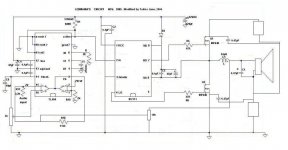
This is standard feature of TL494. Max. duty cycle is 90 % (stated by datasheet), or 80...86 % in reality. If you want 100 %, you have to pull down pin 3 and 4 below zero with a small current.
Oscillator and comparators are what limit duty cycle with TL494, but there is a trick involving a resistor in parallel with a diode and in series with the timing capacitor that improves it... 😀

R=Rt*0,05...0,1. Cathode of diode have to point to IC pin 5.
The schematic in attachment reflects misunderstanding, and won't work at all. Try to analize it! When will one and other FET conduct? Draw waveforms!
And this triangle generator is not too precise.
And those "black boxes" are hiding further problems.
The schematic in attachment reflects misunderstanding, and won't work at all. Try to analize it! When will one and other FET conduct? Draw waveforms!
And this triangle generator is not too precise.
And those "black boxes" are hiding further problems.
It is that thunderball amp split in half. But it may need an error amp on the input in order to work.
the box named level shift is just a regular level shift like in titanchen´s schemo, the thunderball amp dident have a feedback loop so that can be left vacant for now.
the box named level shift is just a regular level shift like in titanchen´s schemo, the thunderball amp dident have a feedback loop so that can be left vacant for now.
... , yes but thunderball amp also works in full bridge topology which does not always require a feedback but in your half bridge case you will need one !
And btw I think that titanchen's level shifter(s) has some issues too so do the revising of your amp again . . .
And btw I think that titanchen's level shifter(s) has some issues too so do the revising of your amp again . . .
- Status
- Not open for further replies.
- Home
- Amplifiers
- Class D
- level shifters and mosfet drivers