Steve Dunlap said:I have not posted my files. I do not use LT4 or any of the other programs I have seen mentioned here.
Just about every simulator out there can export a standard format SPICE netlist, and LTspice can use that as input.
syn08 said:
Steve,
Care to clarify which is correct and final? There's quite a gap here...
http://www.diyaudio.com/forums/showthread.php?postid=1752556#post1752556
Your link references a completely different amp than the one being discussed in this thread. Perhaps that could be the gap?
Steve Dunlap said:
As andy_c proposed: The problem here is that the Vbe's of the outputs do not remain constant. If you make them constant, then you are correct. The Vbe of the "off" device increases as the "on" device conducts more current.
>Third and fourth paragraph: The AC voltage between the emitters of the bias pair remains constant (well very close).<
I guess we need to sit down at a white board.
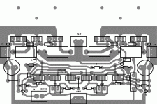
As promised , I just finished my krill PCB artwork. I was waiting
for the masters word , so I guess it is postable.
All this about staying true to the original made me design a
"universal" OPS board.(attached)
A. (on screenshot) are optional basestoppers. Jumper if
not wanted.
B. LED or diode chain - your choice.
C. Even the resistor between OP bases.
D. main bias chain.
E.Optional CCS decoupling.
Servo input to CCS's and choice of either 220u or 470u
main capacitors. I made this for myself, but doubted
whether it would be wanted or appreciated.
It is just the OPS and I will make a stereo SMD VGS
to go with it. If there is any interest ,I will "zip" up a
PCB,BOM,silkscreen package.. if not , I don't need
BOM's or layout guides for this circuit is in my head.
OS
Attachments
andy_c said:
Just about every simulator out there can export a standard format SPICE netlist, and LTspice can use that as input.
Read the rest of my post. Why different results on simulations? Everyone should get the same results if everything is correct, or even incorrect the same way.
I am simply asking the people that believe their simulations are correct to use the same schematic and run their simulation independently. Post your results. If they all agree, I will concede I am wrong. Independently. You can not post one file to be run by several people on the same program. Everyone must do their own.
scott wurcer said:
>Third and fourth paragraph: The AC voltage between the emitters of the bias pair remains constant (well very close).<
I guess we need to sit down at a white board.
I suppose you could look at a DC voltage that varies over time as an AC voltage.
Steve Dunlap said:Read the rest of my post. Why different results on simulations? Everyone should get the same results if everything is correct, or even incorrect the same way.
I am simply asking the people that believe their simulations are correct to use the same schematic and run their simulation independently. Post your results. If they all agree, I will concede I am wrong. Independently. You can not post one file to be run by several people on the same program. Everyone must do their own.
Well, you've claimed that your simulation agrees with the measured distortion data. If that's so, then you're the only one that's solved a problem that's been confounding several people. It would therefore be of benefit for others to see what it takes to get the experimental and simulated data to agree, rather than continue with simulations that do not agree with measured data.
One place to start would be by specifying which models are used for each location, and posting those models in text form.
andy_c said:
Well, you've claimed that your simulation agrees with the measured distortion data. If that's so, then you're the only one that's solved a problem that's been confounding several people. It would therefore be of benefit for others to see what it takes to get the experimental and simulated data to agree, rather than continue with simulations that do not agree with measured data.
One place to start would be by specifying which models are used for each location, and posting those models in text form.
Are you now saying that any small variable can throw the simulation results off?
Using different models certainly can. For example, at a given output stage bias current, two different output device models having beta that varies by a factor of, say, 1.5 will cause the simulated collector currents of the drivers to vary by that same amount (in inverse proportion of course). That's not a SPICE problem per se. It's a matter of making an apples-to-apples comparison.
Steve Dunlap said:Your link references a completely different amp than the one being discussed in this thread. Perhaps that could be the gap?
It could be, but you made several more references to those numbers (links available on request). Could you clarify what amp were you referring to?
Thanks.
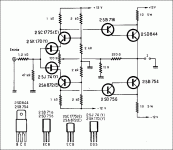
Hi, EDDELARUE,
This crossconduction is the indication of non-turnoff. If you make this crossconduction disappear (by putting R10-100ohm), you are spoiling non-turnoff properties (at higher frequencies) of this circuit.
Could you check simulated THD of 20khz or 50khz signal with and without this R10=100ohm?
This Hiraga amp also don't use base bleeder resistors at base of 2SD844 and 2SB754
during some simulations, I perceived cross conduction between output transistors ( 10kHz and so on....maybe less ). Installing R10=100 as atached file solves that and decreases THD.
This crossconduction is the indication of non-turnoff. If you make this crossconduction disappear (by putting R10-100ohm), you are spoiling non-turnoff properties (at higher frequencies) of this circuit.
Could you check simulated THD of 20khz or 50khz signal with and without this R10=100ohm?
This Hiraga amp also don't use base bleeder resistors at base of 2SD844 and 2SB754
Attachments
Not sure why Steve didn't say it again, but I seem to recall him saying that his computer files for the development of this amp were on a machine that is not operational and is in some sort of state of storage, so not accessible at present.
Let's also try to remember that Steve's in a state of permanent physical disability, ok?
I don't speak for Steve, nor have I discussed this post with Steve, FYI.
I think I also read that the claim for the OS alone was 0.005% but that is from memory.
I don't think the $20 per board is too much... fyi.
_-_-bear
Psssssstttttttttt
<(Be very quiet...I think they're sleeping....
All the people building Steve's amp should sneak over to Krill construction thread - 100W version.
http://www.diyaudio.com/forums/showthread.php?threadid=140056
That way, we could build stuff, share construction tips, troubleshoot, and do things. I know that is the original intent of Steve posting here, he says as much.
All the argumentative, arrogant, egotistical, rude, snarky, theoretical, blathering blabberskites can call this thread home...wielding their fiendish challenges and brandishing their proofs! Their counter-proofs!! "Ah, Ha! Schieskopf!" Rebutals, simulations, contemptous counter simulations--they'll have a ball. They won't even miss us, we should let them argue in peace! Roar at one another! "Gastropod!!!!!!!!!!Did you not read my post eleventy-million!"
(Steve, Ostripper, c2c, and the builders, come on over, I'm a complete blockhead and am gonna need some help, lol!).)>
Nice krill PCB artwork Ostripper!
If anybody's interested in looking at this in more detail in the simulator, try the scenario where the amp is putting out a 5A peak sine wave at 20 kHz. What you'll see is that the voltage difference between the driver bases is constant, but the voltage between the output device bases is far from it. In fact, the voltage difference between the output device bases becomes larger as the amp both sources and sinks high current.
Looking a little closer, one finds that this occurs because it's the inactive driver base-emitter junction, not that of the inactive output device, that takes the brunt of the reverse biasing due to the increased voltage drop across the active output device emitter resistor. The driver is able to turn off very fast because it is driven from a low-impedance source that can provide current to the driver base in both directions. Once a driver turns off, the corresponding output device is left with an open-circuit base. Interestingly, the inactive output device base current goes to zero quite fast, but the emitter current takes a while to decay to zero because of charge storage effects.
That's sort of an interesting aspect of the design that I hadn't noticed before and hadn't seen mentioned before in this thread. If it has been mentioned already, sorry to bring it up again.
Hi, Andy_c,
I also suspected it is the trapped base charge that makes the non-turnoff property in higher frequencies, due to no base bleeder resistor available.
http://www.diyaudio.com/forums/showthread.php?postid=1757353#post1757353
It's interesting because it works in higher frequecies where usually in this higher frequencies, output stage's performance usually declining.
Re: Psssssstttttttttt
I was the 2nd one in the pool! Steve has been there too! Phil H also!
Yes - I'm looking forward to getting some real electrons flowing. Seems as if Andrea has a few to many - but Steve will help put that right I'm sure. 😉
quoydoy said:
(Steve, Ostripper, c2c, and the builders, come on over, I'm a complete blockhead and am gonna need some help, lol!).)>
Nice krill PCB artwork Ostripper!
I was the 2nd one in the pool! Steve has been there too! Phil H also!
Yes - I'm looking forward to getting some real electrons flowing. Seems as if Andrea has a few to many - but Steve will help put that right I'm sure. 😉
lumanauw said:Hi, Andy_c,
I also suspected it is the trapped base charge that makes the non-turnoff property in higher frequencies, due to no base bleeder resistor available.
http://www.diyaudio.com/forums/showthread.php?postid=1757353#post1757353
It's interesting because it works in higher frequecies where usually in this higher frequencies, output stage's performance usually declining.
Bingo! You got it. One can see that the output devices will turn off softly because of this, but what didn't originally hit home for me was the more abrupt turn-off behavior of the drivers.
It's one of those "brain teaser" types of circuits, that's for sure.
Hi Scott,
Did you mean, holding their Vbs constant?
IOW, the transconductance of the output transistors on their own, with 25mA bias, is so non-linear that 50ppm into 8 ohms is not even possible in theory?
Brian
Do you mean, instead, sit down at a water board? Talk about pulling teeth. 😛I guess we need to sit down at a white board.
scott wurcer said:As andy_c proposed take just the output devices running at 25mA and hold their Vbe's constant and alternately source and sink 2.5A there is considerably more than 50ppm of non-linearity at the output. This is basic device physics 101 it has nothing to do with simulators. The voltage at the output can be computed by hand.
Did you mean, holding their Vbs constant?
IOW, the transconductance of the output transistors on their own, with 25mA bias, is so non-linear that 50ppm into 8 ohms is not even possible in theory?
Brian
andy_c said:If anybody's interested in looking at this in more detail in the simulator, try the scenario where the amp is putting out a 5A peak sine wave at 20 kHz. What you'll see is that the voltage difference between the driver bases is constant, but the voltage between the output device bases is far from it. In fact, the voltage difference between the output device bases becomes larger as the amp both sources and sinks high current.
Looking a little closer, one finds that this occurs because it's the inactive driver base-emitter junction, not that of the inactive output device, that takes the brunt of the reverse biasing due to the increased voltage drop across the active output device emitter resistor. The driver is able to turn off very fast because it is driven from a low-impedance source that can provide current to the driver base in both directions. Once a driver turns off, the corresponding output device is left with an open-circuit base. Interestingly, the inactive output device base current goes to zero quite fast, but the emitter current takes a while to decay to zero because of charge storage effects.
That's sort of an interesting aspect of the design that I hadn't noticed before and hadn't seen mentioned before in this thread. If it has been mentioned already, sorry to bring it up again.
I agree with your observations. What are you finding interesting exactly? Is it that, because of the absence of bias resistors at the emitters of the drivers, the drivers BEs are reverse biased rather than the output transistors? (at moderate output currents)
- Status
- Not open for further replies.
- Home
- Amplifiers
- Solid State
- Krill - The little amp that might...