Re: Sounds really good... my Dx Amplifier cannot compete...no chance for my toy!
Dear Carlos - the "Krill" is Steve's attempt to make his design available to the DIY community - and for a low cost. He has the "real deal" at his house - you have seen the photo posted. 90 kilo's and 200W @ 8 oms per channel - balanced output. But - it cost more than twice as much to construct because it has twice as many parts - and even more complex theory of operation. So in some ways Steve is like Papa Nelson - John C - Bear - ASKA - all of these masters of amplifier design don't tell you everything all at once. For one thing there are not to many people that can understand that much information all at once. For another thing it is better to learn in stages and thus appreciate advancing your knowledge of their theory(s). So Steve is showing us things at different levels of design - and he has not shown you everything - yet. Perhaps someday he will - perhaps not. The "big" amplifier is beyond the means and skills of your average DIYer (not being judgmental - just telling it like it is) and thus not many would ever be built - and that gets us more into the discussion end of things instead of the building end of things.
Need to run - the painters need something from me (maybe some $$$ ?)
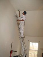
BTW - that is Victor on top of the ladder doing a bit of prep work before the real paint starts going on. It's good that he is young and still able to do these things. The age of my body is beginning to betray me a little with my bad back and bad knee and bad balance. Some would include my bad attitude !!
destroyer X said:
The Krill sounds better... despite my recordings have not shown that (youtube).... into real world you "feel" immediatelly the advantage for Krill.
I was simulating....playing only, as i can do that layed down when i wait the fever temperature to drop (now an infection)... and was not hard to see transistors never switch off...never cut!.... this makes the difference ... one of the best effects (results) you have with class A without all that heat.
I found something i cannot explain...a subproduct.... an offset result of this trick (clever) swing into the output level potential (consequence is a swing)... i found almost 3 volts.... same i found (2.5) when i assembled the first time.... i am not an engineer..also i do not understand electronics so deep to understand..but at least i understood how the amplifier works...beautifull...just beautifull!
I do not think i have an amplifier, now a days, in my home, that can beat the krill..... but will test once more with more guys evaluating.
Be happy.... do not build Dx Amplifier if you want the best possible sound..build Krill!
Dx Amplifier will make you happy..for sure it will...but Krill is better..... CLEARLY BETTER!
regards,
Carlos
Dear Carlos - the "Krill" is Steve's attempt to make his design available to the DIY community - and for a low cost. He has the "real deal" at his house - you have seen the photo posted. 90 kilo's and 200W @ 8 oms per channel - balanced output. But - it cost more than twice as much to construct because it has twice as many parts - and even more complex theory of operation. So in some ways Steve is like Papa Nelson - John C - Bear - ASKA - all of these masters of amplifier design don't tell you everything all at once. For one thing there are not to many people that can understand that much information all at once. For another thing it is better to learn in stages and thus appreciate advancing your knowledge of their theory(s). So Steve is showing us things at different levels of design - and he has not shown you everything - yet. Perhaps someday he will - perhaps not. The "big" amplifier is beyond the means and skills of your average DIYer (not being judgmental - just telling it like it is) and thus not many would ever be built - and that gets us more into the discussion end of things instead of the building end of things.
Need to run - the painters need something from me (maybe some $$$ ?)
BTW - that is Victor on top of the ladder doing a bit of prep work before the real paint starts going on. It's good that he is young and still able to do these things. The age of my body is beginning to betray me a little with my bad back and bad knee and bad balance. Some would include my bad attitude !!
Attachments
Steve
In your boards R9 is connected to ground (0V). The value of 33k is for all versions or only for 50W version? Right now I have a 100K in that place, as the last schematic (100w version).
There is a small problem (easily corrected) with the boards I have. The connection from R14 to Q6 is broken, so we must solder a small wire (underneath and through the defective hole) from end of R14 to emitter of Q6.
Mine is almost assembled!
Cheers
jmmartins said:Steve
There is a small problem (easily corrected) with the boards I have. The connection from R14 to Q6 is broken, so we must solder a small wire (underneath and through the defective hole) from end of R14 to emitter of Q6.
Mine is almost assembled!
Cheers
My boards ohm out OK from R14 to Q6 - although I do see that the PTH near Q6 is missing it's pad on both sides of the PWB. Hmmm - a little bit 22 gauge should fix that. Good Catch!! 😉
Can't wait to hear you findings! 😀 😀 😀
Steve Dunlap said:
I will consider posting that. It will take me a while to draw it up again in my current software.
So, you are willing to accept Charles Hansen's claim, but not mine. May I ask why?
I cannot produce curves of anything. I can not even lift an amp on to my test bench. I know, that is a "convenient" out for me. I really wish I wasn't.
The reason I measured at 20KHz was because another designer told me my measurements at 1K didn't prove anything. If I measured at 20K I would see much higher distortion. I did not. In fact, at all frequencies, at rated power, distortion figures were very low.
I see no way to resolve this if you and others will not accept what I have said. Perhaps someone could come over for a couple of weeks and build one for you (and a couple of others) to test for yourselves. I still have all the parts, except the case to put it in.
Hi Steve,
I don't recall being among those who challenged your claim. I have asked for more information, that is all. Those are two different things.
That other designer was right to ask you to do your distortion measurements at 20 kHz. If you did that and did not see increased distortion, more power to you.
Cheers,
Bob
AKSA said:Distortion figures aside, if Steve's novel output stage manages much lower noise figures, even if only by 10dB and it's likely to be far more than this, then the consequence will be greatly improved resolution which is a very good thing indeed.........
Hugh
I find this a little puzzling. I don't see how the unity gain output stage could contribute to the noise figure in any case. Any triple darlington biased at high currents would have negligible RTI noise. There are cases of power output devices used for even MC preamps their rbb is so low.
You have a 26db VGS in front with at least 40-80nV presented to the output stage.
Hi Bob,
I'm struggling with what appears to be a suspension of reality in this thread. I look at Steve's output stage and can see how the output devices can be reverse biased (switched off) in normal operation. Can you?
Also, do you have any objective understanding of why his saturated transistor bias scheme ought to improve linearity?
Brian
I would be happy if Bob Cordell or other good Christian help me
informing what kind of mistake i have done into simulator...why i am having such crazy off set reading into the simulator... the images posted and text are explaining the subject.
Help me to find my error.... are there a dinamic voltage floating into the output line with ground as reference... are there DC variation there... say...sometimes in a small moment 1 volts positive and them swing to 1 volts negative?
Carlos
Carlos,
I believe we cannot fully accept simulators results. The simulators are dependent on what the software designer put into them and on the accuracy of the data of various components, mainly semiconductors.
I believe we cannot fully accept simulators results. The simulators are dependent on what the software designer put into them and on the accuracy of the data of various components, mainly semiconductors.
simulators
They all got random component spreads,don't they?
Max
ps I don't know,but they must have,surely.
pps Edit] sorry, I realise they must.
They all got random component spreads,don't they?
Max
ps I don't know,but they must have,surely.
pps Edit] sorry, I realise they must.
Re: Re: Sounds really good... my Dx Amplifier cannot compete...no chance for my toy!
Several points here. First, that is 90 lbs, not kilos. The case alone for that amp cost more than twice as much as a pair of the Krill sold for. Then there was the machining, which added time and money. A pair of the Krill use two heat sinks - one each. The 200WPC or the 400W mono use 8 heat sinks each in an assembly created by bolting them together on the 0.188 inch thick side panels. Then there is the difference in transformers - I think you begin to get the picture.
The Krill was designed by me but built by a company that does that sort of thing. Not uncommon in the audio industry. I only built the first two to confirm that they were ready for the first production run.
The larger amps were all built by me. Somewhat more attention to detail was given. All parts were tested and matched. Each channel was tweaked for minimum distortion. The amps used the same transistors, just more of them. There were some other changes also. I used better parts (except transistors) in the large amps. All circuit boards were different with an improved layout and 4oz copper. They were made by a different company that charged much more but did much better work.
I used a different VGS with a different power supply. The amps were fully balanced input to output. I feel that all the small changes combined to make a better sounding amp. They certainly tested better.
As Thomas points out, and we talk on line, by phone and in person so he has had a chance to get to know what I am trying to do, I wanted to present an amp that I knew people could build. I also wanted to explain what I had done and why. Sometimes the teaching part wanders away from construction and dangerously near to the hows and whys of the circuit operation. Hopefully, no one has been put off by that to any great extent. I try to answer questions about both in an informative manner.
Carlos,
I know of at least 12 people currently building the Krill. More people may be building than you realize. If I under stand correctly, ostripper has already built one also, so make that 13.
ostripper has given some valuable insight into how to simulate my circuit. When many people were having trouble with their sim early on, I ask in his Frugal amp thread if he would take a look. He seemed to be comfortable with the simulation process and was getting good results with other designs. He did take a look and he posted what he found. I have not made any attempt to influence what he reports here.
I would also like to thank andy_c for his pointers on running some of the sims more accurately and for his improved transistor models.
One last thing. There is room here for the builders, for those that want to learn something and those that only want to simulate the circuits. I am willing to risk learning something from any of them.
c2cthomas said:
Dear Carlos - the "Krill" is Steve's attempt to make his design available to the DIY community - and for a low cost. He has the "real deal" at his house - you have seen the photo posted. 90 kilo's and 200W @ 8 oms per channel - balanced output. But - it cost more than twice as much to construct because it has twice as many parts - and even more complex theory of operation. So in some ways Steve is like Papa Nelson - John C - Bear - ASKA - all of these masters of amplifier design don't tell you everything all at once. For one thing there are not to many people that can understand that much information all at once. For another thing it is better to learn in stages and thus appreciate advancing your knowledge of their theory(s). So Steve is showing us things at different levels of design - and he has not shown you everything - yet. Perhaps someday he will - perhaps not. The "big" amplifier is beyond the means and skills of your average DIYer (not being judgmental - just telling it like it is) and thus not many would ever be built - and that gets us more into the discussion end of things instead of the building end of things.
Several points here. First, that is 90 lbs, not kilos. The case alone for that amp cost more than twice as much as a pair of the Krill sold for. Then there was the machining, which added time and money. A pair of the Krill use two heat sinks - one each. The 200WPC or the 400W mono use 8 heat sinks each in an assembly created by bolting them together on the 0.188 inch thick side panels. Then there is the difference in transformers - I think you begin to get the picture.
The Krill was designed by me but built by a company that does that sort of thing. Not uncommon in the audio industry. I only built the first two to confirm that they were ready for the first production run.
The larger amps were all built by me. Somewhat more attention to detail was given. All parts were tested and matched. Each channel was tweaked for minimum distortion. The amps used the same transistors, just more of them. There were some other changes also. I used better parts (except transistors) in the large amps. All circuit boards were different with an improved layout and 4oz copper. They were made by a different company that charged much more but did much better work.
I used a different VGS with a different power supply. The amps were fully balanced input to output. I feel that all the small changes combined to make a better sounding amp. They certainly tested better.
As Thomas points out, and we talk on line, by phone and in person so he has had a chance to get to know what I am trying to do, I wanted to present an amp that I knew people could build. I also wanted to explain what I had done and why. Sometimes the teaching part wanders away from construction and dangerously near to the hows and whys of the circuit operation. Hopefully, no one has been put off by that to any great extent. I try to answer questions about both in an informative manner.
Carlos,
I know of at least 12 people currently building the Krill. More people may be building than you realize. If I under stand correctly, ostripper has already built one also, so make that 13.
ostripper has given some valuable insight into how to simulate my circuit. When many people were having trouble with their sim early on, I ask in his Frugal amp thread if he would take a look. He seemed to be comfortable with the simulation process and was getting good results with other designs. He did take a look and he posted what he found. I have not made any attempt to influence what he reports here.
I would also like to thank andy_c for his pointers on running some of the sims more accurately and for his improved transistor models.
One last thing. There is room here for the builders, for those that want to learn something and those that only want to simulate the circuits. I am willing to risk learning something from any of them.
jmmartins said:Steve
In your boards R9 is connected to ground (0V). The value of 33k is for all versions or only for 50W version? Right now I have a 100K in that place, as the last schematic (100w version).
There is a small problem (easily corrected) with the boards I have. The connection from R14 to Q6 is broken, so we must solder a small wire (underneath and through the defective hole) from end of R14 to emitter of Q6.
Mine is almost assembled!
Cheers
R9 should be changed to 33K for the 50W amp and 51K for the 100W amp. That is one of those places having the original files would have saved some revision.
The feed through at that location appears to have no pad. It does have a plated through hole. All the production units were wave soldered and the solder wicked into the hole. You may use a piece on wire through the hole. It will not hurt anything.
lumanauw said:
If we look at the page that Ostripper pointed, http://71.203.210.93/upload/ and read paper "Tanaka_AES.pdf"
So it took Sansui 4 years to make a copy of my patent # 3,995,228
and AES allows publication.
😎
Fine, it is good to know you have 13 building
I have six building here at my Orkut too.
It is all rigth to me...if you want this way...go ahead and be happy.
I will be watching and learning with you.
regards,
Carlos
..................................................................
Thank you Joshua.
Shalom
I have six building here at my Orkut too.
It is all rigth to me...if you want this way...go ahead and be happy.
I will be watching and learning with you.
regards,
Carlos
..................................................................
Thank you Joshua.
Shalom
Bob Cordell said:
Hi Steve,
I don't recall being among those who challenged your claim. I have asked for more information, that is all. Those are two different things.
That other designer was right to ask you to do your distortion measurements at 20 kHz. If you did that and did not see increased distortion, more power to you.
Cheers,
Bob
Perhaps I overreacted a bit. Someone, not you, implied I couldn't accept a little challenge. I became a little angry at first. I am over it now.
So, lets try this again. I used a slightly modified version of the output stage I have posted, with a different VGS in full balanced mode, input to output. Are we still getting hung up on the no GNFB claim?
I agree the other designer was right to ask. I didn't argue, I measured. Maybe it is a good design, maybe I just got lucky. Or as someone, again not you, suggested, maybe I simply don't know how to run the test.
Great!... humble as only the good guys can be
- "Maybe i simply don't know how to run the test"
Perfect Steve!
Carlos
- "Maybe i simply don't know how to run the test"
Perfect Steve!
Carlos
scott wurcer said:
I find this a little puzzling. I don't see how the unity gain output stage could contribute to the noise figure in any case. Any triple darlington biased at high currents would have negligible RTI noise. There are cases of power output devices used for even MC preamps their rbb is so low.
You have a 26db VGS in front with at least 40-80nV presented to the output stage.
26dB? For some reason I thought it was 27.84 dB. Also, my amp is not a triple Darlington biased at high current. You are correct about the noise however.
Since the triple has been brought up so many times, lets look at how my amp performs current wise at low impedance. First, we make the assumption that the current sources providing dive to the output Darlington are set at 10mA as shown. The second assumption is that an amp driving a low impedance load at near maximum current will warm up above ambient temperature. Now look at the spec sheets for the transistors I show on the BOM. That 10mA translates into a maximum output current of 100A, give or take an amp. I really don't expect that from a 16A transistor. Even taking into account beta droop on the output transistor (shouldn't be a problem for the driver) you can easily destroy the transistor before the non triple output stage "chokes" for lack of current.
traderbam said:Hi Bob,
I'm struggling with what appears to be a suspension of reality in this thread. I look at Steve's output stage and can see how the output devices can be reverse biased (switched off) in normal operation. Can you?
Also, do you have any objective understanding of why his saturated transistor bias scheme ought to improve linearity?
Brian
Hi Brian,
I am also having some trouble understanding the output stage, but it does appear to me that the output transistors can be reverse-biased in normal operation.
Cheers,
Bob
Nelson Pass said:
So it took Sansui 4 years to make a copy of my patent # 3,995,228
and AES allows publication.
😎
Hi Nelson,
Hmmmm....
I'll have to take a look at that patent.
Cheers,
Bob
For anyone looking for a US patent, Google has a decent tool:
Google Patent
Much better than the USPTO since the patents can be downloaded or printed in PDF rather the the single page tiffs at the patent office site.
Google Patent
Much better than the USPTO since the patents can be downloaded or printed in PDF rather the the single page tiffs at the patent office site.
Nelson Pass said:
So it took Sansui 4 years to make a copy of my patent # 3,995,228
and AES allows publication.
😎
Think of the money you could have saved by not getting the patent and keeping the design somewhat more private.
I agree that should not have been allowed.
I am also glad you don't keep your designs private. You were one of the people I worried about inevertantly copping when I designed my circuit. Being able to read all your patents and publications was a great relief.
We have met three times at CES. You were a very friendly and open person who spent a great deal of time talking and explaining things. I can't say that about everyone I met there.
- Status
- Not open for further replies.
- Home
- Amplifiers
- Solid State
- Krill - The little amp that might...