I thought this was a KiCAD thread not an abuse Nigel one ?
There is another thread with my software on it if you would like to post there.
I would be happy to deal with your nonsensical questions and claims there.
If KiCAD works for you then fine but dont try to ram it down my throat with your spam !
There is another thread with my software on it if you would like to post there.
I would be happy to deal with your nonsensical questions and claims there.
If KiCAD works for you then fine but dont try to ram it down my throat with your spam !
LOLYour obviously a braver man than me.
Suzy J is much braver than I am 🙂 I call it trail blazing, Go Suzy go, your designs are inspiring to me.
Do not be offend either Nigel, your code does the job, without the bloat and bling
Last edited:
I think you should stop bagging something where it's obvious you've got a clear financial motive to do so..
If you saw my books you wouldnt agree with that statement
No money in software now due to free stuff.
So I design hardware now instead where they dont give it away !
Now can we get back to KiCAD and all its bugs ? you havent answered to that yet.
 This thread is at risk of derailing and it needs to return to it's topic without delay (Rule #1). If there is any doubt as to what that is, please go and re-read the first post.
Dude you are completely out of line.. I understand your agenda, take it elsewhere.Personally I saw it as gross spam and was offended by it.
You can also export KiCAD PCB into 3D in FreeCAD with KiCADStepUp plugin installed, it works great. The small PCB on top has been exported with KiCADStepUp
Now that’s amazingly cool. One of the things I’ve been toying with for power amps is doing a main board with all the hoofer power transistors, and a daughter board that sits on top with the low-current front end. I could create a footprint for the low-current bit, and export the whole PCB of it for the 3D render.
Mind blowing. I’d never contemplated boards as components.
That is exactly what I think - but did not write hereIt was, until you barged in.
Sorry Nigel, but you trying to compare your product with KiCad is laughable. I haven't tried to run your CAD system, but I can tell from the screen grabs on your webpage that it's firmly stuck in 1993. I used to run Protel AutoTrax and Schedit on DOS machines, and it looked remarkably similar. Big, chunky graphics that were optimised for EGA and VGA. Text based menus, because they're quick and easy to code. No fonts, so your silkscreens and schematics come out barely legible.
The screen-grabs you show for your product do nothing for it. The PCB you feature is the sort of thing that, had one of my techs produced it, I'd have spent some time with them teaching them how to design a decent board. Little things, like bevelling corners at 45 degrees (and sticking to 45 and 90 degree tracks unless there's a good reason not to), honouring minimum feature size for via annular rings, not having acute angles where tracks join. Cleaning up after you've done a copper pour so there's no mess.
And your schematics are barely readable. The whole idea of design is to make something that's manufacturable and maintainable, and those designs you show are neither.
KiCad, on the other hand, creates very manufacturable boards, and really beautiful schematics. I've attached a couple of screen-grabs from the board I'm currently working on. It's a dense little guy, with a whole lot of transistors, but that's how I like to do things. KiCad makes the job of producing a really clean schematic and layout straightforward.
I think you should stop bagging something where it's obvious you've got a clear financial motive to do so. We get you're bitter. Now rack off please.
And by the way, this is a KiCAD thread so who is the spammer here?
Now that’s amazingly cool. One of the things I’ve been toying with for power amps is doing a main board with all the hoofer power transistors, and a daughter board that sits on top with the low-current front end. I could create a footprint for the low-current bit, and export the whole PCB of it for the 3D render.
Mind blowing. I’d never contemplated boards as components.
You can even place an enclosure around your PCB - or at least a partially open enclosure, otherwise you won't see the inside of it 🙂 Did that with a custom fooprint which has only a crosshair on the fab layer and the step model of the enclosure attached to it. You can move the enclosure around with x/y/z offsets and rotation.
Very helpful for checking clearance issues, placement of knobs, connectors etc. on front plates and so forth.
Nigel, free software can exist together with commercial SW. Open/Libre Office is free, and MS sells still a lot of Office packages. Would I use KiCad professional, no. But for hobby it is great SW. Nigel, please don’t try to change this tread in a KiCad bashing tread. KiCad, for what it is intended, is quite good.
There is money to be made selling auxiliary software for KiCad.Nigel, free software can exist together with commercial SW. Open/Libre Office is free, and MS sells still a lot of Office packages. Would I use KiCad professional, no. But for hobby it is great SW. Nigel, please don’t try to change this tread in a KiCad bashing tread. KiCad, for what it is intended, is quite good.
For example, there are many users who would pay a reasonable price for a better autorouter than FreeRouting, better layer control, net priority and please not in Java.
One reason for FreeRouting and its forks going nowhere fast has been the effort required to keep up with Oracle Java, OpenJDK and Zulu changes
KiCad itself does not use Java
KiCad itself does not use Java
Anybody tried the "replicate layout" plugin?
GitHub - MitjaNemec/Kicad_action_plugins: Kicad action plugins
It works like a charm for any hierarchical sheet which layout you only want to do once and then simply copy.
Using 5.1.6 and there seem to be no flaws.
GitHub - MitjaNemec/Kicad_action_plugins: Kicad action plugins
It works like a charm for any hierarchical sheet which layout you only want to do once and then simply copy.
Using 5.1.6 and there seem to be no flaws.
Last edited:
I would love to use the replicate layout tool. But I'm just learning KiCad and I don't know how to add this plugin. Could someone detail, step-by-step, how to enable this tool in KiCad 5.1.6?
I will second the request for a tutorial on the "replicate layout" plugin.
That's also a feature that I and many others would use every single day if it was integrated into KiCAD by default.
So often I'll have a board that has something like 10+ Versalink fiber inputs and almost as many outputs. A "replicate layout" function would make that much quicker to deal with. Normally what I do is copy, paste, then manually change the component designators. That's a lot of work for a complicated layout to be replicated.
People here would probably use it since we're typically dealing with stereo systems.
It´s all described at the link I posted.
Download the "replicate layout" folder and put in the "scripting" folder;
wherever this might be on your PC.
Then you are basically good to go.
(it´s now under tools/external plugins)
Place a hierarchical sheet in your schematic (something that is used multiple times). If you have a final version of that sheet, do the layout.
Then place another sheet in the schematics.
Annotate, update PCB and do as described in that link above.
Haven´t played around with it extensively but started a design for a discrete crossover which is basically a little buffer with some passives around, copied about a dozen times.
It works really nice. Copies all the tracks and vias.
Last edited:
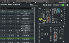
Here’s a cool one. There’s a tool for KiCAD that does interactive assembly placement. Just run it from the PCB window and it creates a HTML file with all your components, ordered by type. So then when you hover over a component in the list, it highlights all the spots on the PCB where it goes, top and bottom.
It makes assembly too easy, I reckon, especially where your boards are dense enough that you can’t fit the designators into the silkscreen.
And when you’re assembling, you don’t even need KiCad. Just the htm file and a browser.
It makes assembly too easy, I reckon, especially where your boards are dense enough that you can’t fit the designators into the silkscreen.
And when you’re assembling, you don’t even need KiCad. Just the htm file and a browser.
Attachments
- Home
- Design & Build
- Software Tools
- KiCad 5.1