@Mello4, have you found the FAQ section of the KiCad Forum? I'm not sure how complete it is, but I know there are a lot of Cliff-notes type stuff in it.
I had been looking at the documentation here: Documentation | KiCad
This looks a lot more useful for KiCad info:
(Start Here) Frequently Asked Questions - FAQ - KiCad.info Forums
The software puts libraries in various places. I just am trying to figure out the proper directory & file structure on Win 10.
There seem to be libraries here C:\Program Files\KiCad\share\kicad\library
There are some libraries here C:\Program Files\KiCad\share\kicad\modules
The Mouser 'Library Loader' is a bit obtuse.... ms.componentsearchengine.com/pcb-libraries.php
I have a project under /PCB-Board-Design/xxx
Not sure which library location is correct of these two?
I have these libraries under /PCB-Board-Design/CAD-Model/
/SamacSys_Parts.3dshapes
/SamacSys_Parts.pretty
/xxx-pcb-part-libraries
Also model files/
xx.bck
xx.dcm
xx.lib
xx.mod
xx.kicad.mod
xx.epc
xx.stl
xx.stp
xx.wrl
xx.epw
I also have these libraries under /PCB-Board-Design/CAD-Model/KiCAD/
/SamacSys_Parts.3dshapes
/SamacSys_Parts.pretty
Also model files/
xx.bck
xx.dcm
xx.lib
xx.mod
xx.kicad.mod
Treat libraries from 3rd parties just like those you make yourself and DO NOT put them in the Progam Files location. Every time you upgrade KiCad the built in libraries get overwritten
Treat libraries from 3rd parties just like those you make yourself and DO NOT put them in the Progam Files location. Every time you upgrade KiCad the built in libraries get overwritten
I did not put any libraries under Program Files location. I searched for where library locations may exist.
I was trying figure out what location the program prefers to put the user libraries.
My PCB directory for projects is under /PCB-Board-Design/xxxxproject/
One of these library locations is wrong...
I now have some libraries under /PCB-Board-Design/CAD-Model/
and some libraries under/PCB-Board-Design/CAD-Model/KiCAD/
I think I found some answers here: Where are the configuration files (settings, library tables)? - FAQ - KiCad.info Forums
It seems at startup of KiCAD sets the user library defaults here on Win 10:
C:\Users\AppData\Roaming\kicad\kicad_common
C:\Users\AppData\Roaming\kicad\sym-lib-table
C:\Users\AppData\Roaming\kicad\fp-lib-table
It seems at startup of KiCAD sets the user library defaults here on Win 10:
C:\Users\AppData\Roaming\kicad\kicad_common
C:\Users\AppData\Roaming\kicad\sym-lib-table
C:\Users\AppData\Roaming\kicad\fp-lib-table
KiCad has no particular preference for user libraries location that I am aware of - you can put them anywhere you would like. Mine reside in the a few folders in the documents folder.
Ultralibrarian and Library Expert all support KiCad, both Mouser and DigiKey have links to Ultralibrarian symbols and footprints for some of the components they sell. You do need to have a free account to access them.
Ultralibrarian and Library Expert all support KiCad, both Mouser and DigiKey have links to Ultralibrarian symbols and footprints for some of the components they sell. You do need to have a free account to access them.
KiCad has no particular preference for user libraries location that I am aware of - you can put them anywhere you would like. Mine reside in the a few folders in the documents folder.
Ultralibrarian and Library Expert all support KiCad, both Mouser and DigiKey have links to Ultralibrarian symbols and footprints for some of the components they sell. You do need to have a free account to access them.
I found the settings that control the library default, which can be either global or specific project device PCB models. The key was to find this webpage for the answers.... (Start Here) Frequently Asked Questions - FAQ - KiCad.info Forums
Mouser seems to recommend Library Loader (which I find obtuse): Easy Way to Get Symbols, PCB Footprints & 3D Models | Mouser
"How to use the Schematic Symbols and PCB Footprints:
- Install Library Loader - The PCB Part Libraries require FREE Library Loader software to convert them into your ECAD tool format.
- Run the Library Loader from its desktop shortcut.
- Open your ECAD tool, and the libraries will already be loaded automatically.
- When browsing Mouser's parts, simply click the component ECAD Model symbol from the Mouser site and drop it into your design. Once selected, the schematic symbols, PCB footprints and 3D models are immediately available for use and placement.
- If a part doesn't have a symbol or footprint when clicking on the icon to download, you can build one or request a part. To build, simply use the wizard from SamacSys to create both the schematic symbol and PCB footprint. To request a part, fill in the required information, including your email, and SamacSys will contact you once their engineering team has completed the build."
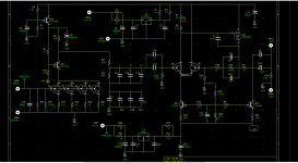
I was hoping someone here might be able to assist me with some errors i am receiving when I run the ERC check. Some errors are listed below.
I have also attached the complete error log (needed to rename to .txt)along with an archived copy of the work.
Kicad ver: 5.1.9
Schematic is of the Pass Pearl 2.
Any help would be great.
Thanks, James
***** Sheet /
ErrType(12): Different net assigned to a shared pin in another unit of the same component
@(132.08 mm, 40.64 mm): Pin ~ on U1 is connected to both Net-(C3-Pad1) and Net-(C1-Pad1)
ErrType(3): Pin connected to other pins, but not driven by any pin
@(132.08 mm, 40.64 mm): Pin ~ (Power input) of component U1 is not driven (Net 2).
ErrType(3): Pin connected to other pins, but not driven by any pin
@(129.54 mm, 152.40 mm): Pin ~ (Power input) of component U2 is not driven (Net 5).
ErrType(12): Different net assigned to a shared pin in another unit of the same component
@(172.72 mm, 96.52 mm): Pin ~ on Q4 is connected to both Net-(C12-Pad1) and Net-(Q10-Pad1)
Attachments
The errors seem to follow Pad symbol naming values. For example at the input of R1 and R2 to U1 you have a symbol Pad1 +Dc in and another symbol +vdc at the same junction point, kicad errors are indicating you have two nodes of different functions connected to each other, best thing to do is delete one of the symbols.
The same error also exists on the gnd pin of U1 where you have a symbol GND and another symbol labelled Pad2 ground connected to the same node, you'll need to delete one of the symbols, keeping the GND symbol would be preferable.
The same types of errors are at U2 Vin, the input Pad5 / Pad6 and Pad4.
I made some amendments to your schematic as an example of the changes you can refer to.
Attachments
Indiglo,
Thank you very much for your time. I will download this information and see what you changed.
The other thing I just found was that the components need pin numbers; at least according to one page I ran across. I will see if I can find that in the manual.
This is my first time with this type of software and figured I would hit a few bumps somewhere.
Thanks again, James
I suspect its because of the footprint being used. Kicad has standard footprints you may want to use those instead. For example the jfets are probably TO92, select the appropriate jfet footprint symbol from the kicad library that matches the pinout of the real jfet, if you make a pinout error because of a wrong footprint in the schematic it will carry over into the pcb layout.
Aim65,
Thank you, I did not catch that error.
I just realized (been sick the past couple of days); that I had left any G-S-D symbols in the schematic. My intention for this was just to basically copy Wayne's schematic but make some changes to some capacitors to have some boards made up for myself.
Since I have purchased the boards from Pass years ago I wanted to try some different caps which have different physical footprints than the original design; which in turn lead me to download and try out this software. Hopefully if anyone was going to make their own PCB's they would go straight to the source for the data.
Newbie question finding component footprints
I'm trying to learn Kicad by modifying an existing project that a member has kindly posted on this site, namely Jeff Young's F3 PCBs.
I want to change the component footprint for one of the power semi's in the design. With a through-hole adapter made available in the Lu1014 GB thread, I figured I could just change the Lu1014 footprint to match those for the IRFP240s already used in the project and get by with a quick and dirty solution.
But I get the following error when I try to change the footprint for the Lu1014:
I'm guessing it's because the specified footprint was custom created by Jeff in his initial design, and so it's not in the standard footprint library for Kicad. I'll be going through Kicad's documentation next to try and figure out how to resolve this error message, but figured I might get a faster answer by asking in this forum.
Thanks (in advance),
Dan
I'm trying to learn Kicad by modifying an existing project that a member has kindly posted on this site, namely Jeff Young's F3 PCBs.
I want to change the component footprint for one of the power semi's in the design. With a through-hole adapter made available in the Lu1014 GB thread, I figured I could just change the Lu1014 footprint to match those for the IRFP240s already used in the project and get by with a quick and dirty solution.
But I get the following error when I try to change the footprint for the Lu1014:
Error: Update footprint “Q2” (from “TO_SOT_Packages_THT:TO-247_Horizontal_Heatsink”) to “TO_SOT_Packages_THT:TO-247_Horizontal_Heatsink”: *** footprint not found ***
I'm guessing it's because the specified footprint was custom created by Jeff in his initial design, and so it's not in the standard footprint library for Kicad. I'll be going through Kicad's documentation next to try and figure out how to resolve this error message, but figured I might get a faster answer by asking in this forum.
Thanks (in advance),
Dan
Are you using 5.1 or 5.99? (If 5.1, switch now. 5.99 is much better.)
Do an 'Ctrl+E' ('Cmd_E' on Mac) over one of the IRFP240s. It should open it in the Footprint Editor. Now do a save-as to whatever library you want to put it in.
Now you can update the Lu1014 (and all the IRFP240s) to point to that library entry.
Do an 'Ctrl+E' ('Cmd_E' on Mac) over one of the IRFP240s. It should open it in the Footprint Editor. Now do a save-as to whatever library you want to put it in.
Now you can update the Lu1014 (and all the IRFP240s) to point to that library entry.
- Home
- Design & Build
- Software Tools
- KiCad 5.1