Well, not strictly true, since RDSon is measured in the triode region (Vds < (Vgs - Vth)) but a MOSFET in a capacitance multiplier operates in the pentode region (Vds > (Vgs - Vth)).lAlso look at the Rdson value. Lower equals better multiplier performance.
The parameter that actually matters is the transconductance, gm, which is the slope of the Vgs versus Ids curve: gm = dIds/dVgs. Higher gm means better performance, since a source follower's output impedance Zout equals (1/gm).
However it is often, but not always true, that MOSFETs with low RDSon also have high gm. Searching for MOSFETs with low RDSon will often discover devices that also have high gm, which is what you want. I recommend narrowing the list down to a half dozen candidates, then actually opening their datasheets to find their gm values.
You're right, but it's much easier to achieve that Vds > (Vgs-Vth) condition when Rdson * Id is maintained to a low level for any/all output current conditions.
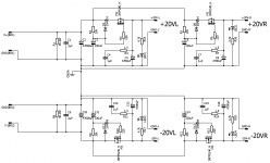
Vds in the multiplier as shown is very low, because there is no resistor defining the gate voltage as a proportion of the input voltage. Vgate = Vinput after averaging the input ripple.
Vds in the multiplier as shown is very low, because there is no resistor defining the gate voltage as a proportion of the input voltage. Vgate = Vinput after averaging the input ripple.
One option is to use an external monolithic bridge (center bolt with 4 spades), in which case we could add some clever jumpers at the appropriate diode holes and connect the DC input to the AC spades. But for Class AB operation, the setup as is will be just fine.
Here is an option with just removing the diode bridge and keeping everything same. As you mentioned, the diode bridge can be external '35A chassis mount' ones. Although this arrangement can be made with earlier layout as suggested by you.
Attachments
Last edited:
That looks very slick, Prasi. Perfect! When you think it's ready please post Gerbers. The other advantage with external bridge is cost effectiveness. Those MUR880 TO220 diodes are $1ea - about same price as IRFP240 in quantity.
Thanks,
X
Thanks,
X
Last edited:
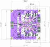
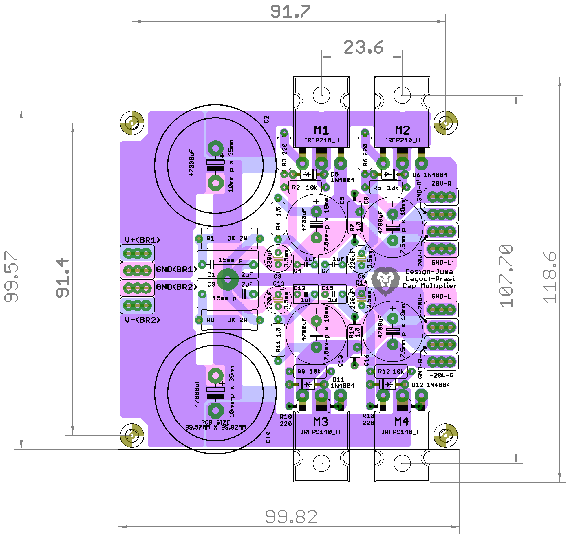
Very neatly done, Prasi - and all inside 16 sq inches!
I wonder what "ammel'" has in mind regarding some changes?
Maybe next time, move the central ground point to the output away from the charging caps and their 'noise', particularly for the filter caps - this then becomes the new 'central ground point', not near to the diode/ripple cap point - a bit of a contentious point in some circles, I think
Maybe also, could shift a couple components to mount underneath (or 'piggyback' a couple [ie, R1 and C1], or SMD some larger size resistors) to free up enough room for the return of the AC snubbers, and maybe leds for 'working' indicators ...
Just saying, no criticism
I haven't found a need for massive capacitance on my own design amplifier power supplies.
I always decouple my amplifier front ends so there is virtually no hum from the power supply.
A 56R and 100uF decoupling is a lot cheaper than thousands of microfarads of electrolytic.
I always decouple my amplifier front ends so there is virtually no hum from the power supply.
A 56R and 100uF decoupling is a lot cheaper than thousands of microfarads of electrolytic.
Jonathan,
You are 100% correct. That's all there is to it. Just keep in mind that a mosfet like IRF610 will drop about 4v from input to output. So size the upstream PSU appropriately to get desired voltage downstream. An SMT mosfet like ZVN4306 drops only about 3v. An IRFP240 can drop as much as 4.5v.
look at the Idmax value
610 =3.3A, 620 =5.2A, 630 = 9A, 510 =5.6A, 520 =9.2A
These have to be derated depending on the FET temperature. Compare the 100degreesC to the 25degreesC values.
Also look at the Rdson value. Lower equals better multiplier performance.
Thank you both. I have finished building mine with the IRF610, and wired it with my test rig, using a 12V SMPS. At the output it measures 12.02V and after the CM it's down to 7.5V. So mine eats up 4.5V 😀😀 greedy little bugger.
I haven't really paid any attention to sound quality, rather, I'm just letting it run before I move it to my main rig, that has 15.75V at the output. I think I can live with 11VDC for a while.
Try 19v SMPS upstream of Cx for 14.5vdc - perfect for TDA7297 I think. Photos?
Lovely work, Prasi, you are getting better and better.......
Congratulations!!
HD
+1, Prasi is a master of layout, and he gives us all of this for FREE! Bravo.
Thank you, Prasi!
It should be pointed out that this slick 100mm square circuit, connected to a trafo with two secondary windings (a standard config of trafos), now gives essentially qnty 4x isolated power supplies because the power fluctuations on one is independent of another now, so the two amp boards will see essentially a dual mono-block PSU for super channel separation. All this without expense of second trafo, second CRC PSU, etc, and better overall ripple suppression as if the caps were huge 200mF deals.
Very neatly done, Prasi - and all inside 16 sq inches!
Maybe next time, move the central ground point to the output away from the charging caps and their 'noise', particularly for the filter caps - this then becomes the new 'central ground point', not near to the diode/ripple cap point - a bit of a contentious point in some circles, I think
Maybe also, could shift a couple components to mount underneath (or 'piggyback' a couple [ie, R1 and C1], or SMD some larger size resistors) to free up enough room for the return of the AC snubbers, and maybe leds for 'working' indicators ...
Just saying, no criticism
HI James,
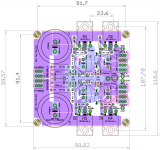
Thank you for your suggestions. Reworked the layout, see attached. Is this what you are suggesting when you say 'move central gnd to output'. By moving to o/p side, It now almost looks like a proper layout for LM317/337 type ckt. Should cap multipliers too should get their ground reference from o/p?
Added 3mm LED indicators, with smd resistor on bottom. I am trying to avoid SMD especially high power components (R1/R8) as they are not easily available locally.
Lovely work, Prasi, you are getting better and better.......
Congratulations!!
HD
Thank you Hugh, Cheers! I am hoping its useful to many people.
regards
Prasi
Attachments
Cool circuit. I've always used a very similar ckt the only difference being a resistor to GND from the 10kohm to the gate since I always thought I needed to drop the gate slightly from Vrail to ensure compliance. Didn't know this is what is called a cap-multiplier.
This site is simply awesome. Always something to learn.
MOSFETs with low RdsON always have higher parasitic capacitances than FETs with higher RdsON. Since you are not operating with the MOSFET in the 'ON' state, but rather linearly, the RdsON is pointless to use when selecting FETs.
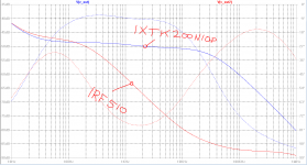
Tho this is a follower, the high capacitance of a powerful FET such as IXTK200N10P will give poorer attenuation with frequency than a light-weight FET such as IRF510.
Todays FETs are unfortunately made to switch fast in SMPS service and are not as good in linear circuits (such as for pass duty in regulators). Even todays IRF610s or IRF240s are probably not as robust as same parts 10years ago. But they switch better.
I'd look for low capacitances and large package when selecting FETs for this duty.
This site is simply awesome. Always something to learn.
MOSFETs with low RdsON always have higher parasitic capacitances than FETs with higher RdsON. Since you are not operating with the MOSFET in the 'ON' state, but rather linearly, the RdsON is pointless to use when selecting FETs.
Tho this is a follower, the high capacitance of a powerful FET such as IXTK200N10P will give poorer attenuation with frequency than a light-weight FET such as IRF510.
Todays FETs are unfortunately made to switch fast in SMPS service and are not as good in linear circuits (such as for pass duty in regulators). Even todays IRF610s or IRF240s are probably not as robust as same parts 10years ago. But they switch better.
I'd look for low capacitances and large package when selecting FETs for this duty.
Attachments
The important figure is how much ripple attenuation at line AC frequency of 50Hz/60Hz. I seem to recall about -50dB when I ran the LTSpice sim for this with IRFP240 and also added an LC filter at the output. -50dB makes a huge difference with hum suppression though.
The important figure is how much ripple attenuation at line AC frequency of 50Hz/60Hz. I seem to recall about -50dB when I ran the LTSpice sim for this with IRFP240 and also added an LC filter at the output. -50dB makes a huge difference with hum suppression though.
True that. But isn't it 100/120Hz? or are we using half wave rectification?
When you analyze the circuit to discover the reason why some of the 60Hz / 120Hz input appears on the output,
you may agree with me that the easiest way to improve this is to cascode the output stage.
And if you are determined to use MOSFETs, you may agree with me that the headroom considerations disappear when you give yourself permission to build a dickson charge pump.
you may agree with me that the easiest way to improve this is to cascode the output stage.
And if you are determined to use MOSFETs, you may agree with me that the headroom considerations disappear when you give yourself permission to build a dickson charge pump.
When you analyze the circuit to discover the reason why some of the 60Hz / 120Hz input appears on the output,
you may agree with me that the easiest way to improve this is to cascode the output stage.
And if you are determined to use MOSFETs, you may agree with me that the headroom considerations disappear when you give yourself permission to build a dickson charge pump.
Sorry man, I havent read the whole thread. The interesting part is the simple cap-multiplier. The more intricate ckts look more like voltage regulators to me.
My intention was to give my dime (inflation so no longer 2cents) ragarding MOSFET selection.
Sorry if I jumped in and interupted, the thread has probably evolved way past the simplest C-x.
When you analyze the circuit to discover the reason why some of the 60Hz / 120Hz input appears on the output,
you may agree with me that the easiest way to improve this is to cascode the output stage.
And if you are determined to use MOSFETs, you may agree with me that the headroom considerations disappear when you give yourself permission to build a dickson charge pump.
Please show us how to make such a device with charge pump, cascode, and low dropout. I'm all ears. I hope it works easily though as the Juma circuit is one of the few that never fails to work, albeit, with large dropout voltage. I have tried building more complex 2 BJT based cap Mx before. They just failed to even work. Maybe just me not properly making circuit?
First do an analysis and discover why some of the sinusoidal input, finds its way onto the output; why isn't there infinite attenuation?
You might determine that infinite amounts of bypass capacitance on the MOSFET gate, does not translate into infinite amounts of attenuation (figure 1). Or, you might discover that I am completely misguided and totally wrong. If so then my claim "cascodes make it better" becomes highly dubious.
_
You might determine that infinite amounts of bypass capacitance on the MOSFET gate, does not translate into infinite amounts of attenuation (figure 1). Or, you might discover that I am completely misguided and totally wrong. If so then my claim "cascodes make it better" becomes highly dubious.
_
Attachments
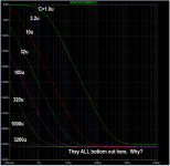
That's a useful plot because it says if we just want to attenuate 60Hz hum, anything larger than 30uF doesn't but you anything.
Very few things are infinite. Might even be something like a limit of an infintite wall to quantum tunneling. In this case the intrinsic blocking of a hexFET mosfet is -45dB.
Very few things are infinite. Might even be something like a limit of an infintite wall to quantum tunneling. In this case the intrinsic blocking of a hexFET mosfet is -45dB.
+1, Prasi is a master of layout, and he gives us all of this for FREE! Bravo.
Thank you, Prasi!
It should be pointed out that this slick 100mm square circuit, connected to a trafo with two secondary windings (a standard config of trafos), now gives essentially qnty 4x isolated power supplies because the power fluctuations on one is independent of another now, so the two amp boards will see essentially a dual mono-block PSU for super channel separation. All this without expense of second trafo, second CRC PSU, etc, and better overall ripple suppression as if the caps were huge 200mF deals.
Thank you x,
here are the schematic, stuffing guide and gerbers. LED resistors mount from bottom.
regards
Prasi
Attachments
- Home
- Amplifiers
- Power Supplies
- Juma's Easy-Peasy Capacitance Multiplier