Dear Mr. MikeW,
Maybe better change to 2sk170BL and 2sj74BL for all user easy to buy ?
regards walter
Maybe better change to 2sk170BL and 2sj74BL for all user easy to buy ?
regards walter
MikeW said:1. Drain 1
2. Gate 1
3. Source 1
4. Substrate
5. Source 2
6. Gate 2
7. Drain 2
If you need the data sheets send me an e-mail
The layout still needs to be checked.
You should be able to put them in the existing holes.
Hallo MikeW, it's possible for a symetric input on your pcb?I would be join with 10-12 stereo sets.
regards walter
regards walter
john curl said:Caps MUST be polypropylene, mica, better. Big problems here with this layout.
New layout coming.
I've got the second variation of the front end for my all-FET version up and running. It's working scary-well as a stand-alone. It'll be a few more days before I get an opportunity to hook it to an output stage.
As far as the DIY-friendliness factor, that remains the same. Build Mike's. Mine takes a lot of hard-to-get parts and you have to buy lots of them so you can match. Then you've got to trim things in with pots. Mike's will be a lot easier to get along with.
(Plus he's easier to get along with than I am, but I'm not going to admit that out loud.)
Grey
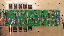

Fixes so far.
The cap for the zobel is too big and the output inductor is too small.
We are getting closer.😀
The cap for the zobel is too big and the output inductor is too small.
We are getting closer.😀
Much better layout! Good work Mike!
🙂
Thanks for implementing some of my previous ideas.
Looks like you have added a cap, C9, yes?
Could you maybe update the schematics with the correct schematic symbols and all values?
Some comments on the layout:
a) How about adding a screw hole in the middle of the PCB for increased stability?
b) Would be nice to have another GND connector next to the output GND.
c) The pad for C8 looks a bit too small. What type of cap did you have in mind here?
d) The wire connection that is just above "R3" looks a bit weird.
e) As you noted yourself, C7 and L1 should have other sizes. L1 could actually have the pad size of the pad for C7, and vice versa.
f) I would like to have a smaller cap (~10-100n PP) in parallel with the 100uF caps just next to these bigger caps to stop noise/RF from entering the board wirewise
What do you think, Mike?
Sigurd
Sigurd Ruschkow said:Much better layout! Good work Mike!
🙂
Thanks for implementing some of my previous ideas.
Looks like you have added a cap, C9, yes?
Could you maybe update the schematics with the correct schematic symbols and all values?
Some comments on the layout:
a) How about adding a screw hole in the middle of the PCB for increased stability?
b) Would be nice to have another GND connector next to the output GND.
c) The pad for C8 looks a bit too small. What type of cap did you have in mind here?
d) The wire connection that is just above "R3" looks a bit weird.
e) As you noted yourself, C7 and L1 should have other sizes. L1 could actually have the pad size of the pad for C7, and vice versa.
f) I would like to have a smaller cap (~10-100n PP) in parallel with the 100uF caps just next to these bigger caps to stop noise/RF from entering the board wirewise
What do you think, Mike?
Sigurd
a. not needed
b. It has 2 holes for ground.
c. 5-10 pf
d. It will work
e. yes
f. I'll think about that one.
MikeW said:latest schematic🙂
Thanks, Mike.
C9 should be connected after R9 if you want it to work as part of an RC LP filter removing RF. Now it is before R9.
Sigurd
- Home
- Amplifiers
- Solid State
- John Curl amp