Member
Joined 2009
Paid Member
The modification is around the Voltage Amp stage: changing that to a simple Sziklai pair with unity gain, drops the distortion down from 0.09% to 0.03%, which is quite good, however it starts to rise a bit at about 20KHz to about 0.07%
Hi Mike,
Nice build!
The circuit diagram you posted is not a Sziklai pair, the one transistor has the base and emitter shorted together ?
I also tried the Sziklai as the VAS in my JLH '69 amplifier and I didn't like the sound so I took it back out. It was lower distortion perhaps but it lost the 'magic', became almost harsh to my ears. In fact the sound reminded me of when I used Sziklai pairs to build an LTP input stage (my TGM2 amplifier) - the distortion was lower than the simple LTP (my TGM1 amplifier), the bass was stronger (less 2nd harmonic no doubt), but the sound was not nice in the treble.
Since you had a good experience with the Sziklai there must be some limitations in my implementation of it that I don't yet understand.
http://www.diyaudio.com/forums/solid-state/268846-tgm9-my-version-jlh-69-class-amplifier.html
Last edited:
Hi mjona
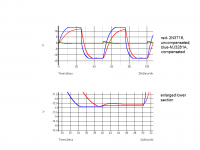
Here are some simulation pictures.
Paraphrasing Doug Self it is probably cruel to subject a JLH10-watter to a 20kHz square wave with a 1 uF load (in parallel withh 8 ohms).
The "original" circuit (2N3716 output) shows a high degree of asymmetry. On the rising edge, the slew rate is limited by the bootstrapped 3716. It does not even reach the peak output voltage in the half-period. On the falling edge, the response is quicker (hence my earlier point that a driver in front of the output device can help).
The 3281a output stage is faster - the peaks are reached within 10us, but the rising edge is still limited by the output's own bootstrap pull-up.
Looking at the second image the negative output signal shows a "transient" overshoot on both but the effect is worse on the 3716 variant.
I have a concern that a good transient performance could be worse if an additional RC network is added since this makes a 4 ohm load (or thereabouts) whereas the JLH amplifier is current limited (to the standing current), unlike a class AB amp.
The other point to note is that the central traces plot the emitter-base voltage of the input transistor. Clearly during the rising edge of the output the transistor is completely cut off. This is in fact the origin of Otala's "transient intermodulation distortion". It affects both amplifier variants but the 3821A model recovers more quickly. Whether real life signals cause this or not is an open question that I have not seen fully addressed. The moral of this story is don't use capacitor speakers!
If a good transient response is needed for 20kHz (and probably isn't) into a capacitive load the standing current would have to be in the order of 20A.
I re-read JLH's original article and the only square wave signal published that I saw was the 50 kHz resistive load. There is a very slight overshoot in the 3821A variant but this does reduce with a slightly larger compensation capacitor (e.g. 47pF). I would still recommend 33pF as this seemed to be the smallest my actual amplifiers were happy with.
John
Attachments
Hi Mike,
Nice build!
The circuit diagram you posted is not a Sziklai pair, the one transistor has the base and emitter shorted together ?
I also tried the Sziklai as the VAS in my JLH '69 amplifier and I didn't like the sound so I took it back out. It was lower distortion perhaps but it lost the 'magic', became almost harsh to my ears. In fact the sound reminded me of when I used Sziklai pairs to build an LTP input stage (my TGM2 amplifier) - the distortion was lower than the simple LTP (my TGM1 amplifier), the bass was stronger (less 2nd harmonic no doubt), but the sound was not nice in the treble.
Since you had a good experience with the Sziklai there must be some limitations in my implementation of it that I don't yet understand.
http://www.diyaudio.com/forums/solid-state/268846-tgm9-my-version-jlh-69-class-amplifier.html
hi Bigun,
Yes you are correct, the diagram is wrong, the correct one has the collector of the npn connected to the base of the pnp with the 560R from the pnp's base to it collector. My mistake.
I have yet to listen to this latest version on my matrix 801s: I've been listening to it on some old Celestions in my workshop. The current version I am using with the 801s is the Geoff Moss high power circuit which I find very impressive as I said in my previous post.
I'll report back when I have retrofitted the new circuit to one channel and done an A/B comparison.
Kind regards
Mike
Hi mjona
Here are some simulation pictures.
Paraphrasing Doug Self it is probably cruel to subject a JLH10-watter to a 20kHz square wave with a 1 uF load (in parallel withh 8 ohms).
The "original" circuit (2N3716 output) shows a high degree of asymmetry. On the rising edge, the slew rate is limited by the bootstrapped 3716. It does not even reach the peak output voltage in the half-period. On the falling edge, the response is quicker (hence my earlier point that a driver in front of the output device can help).
The 3281a output stage is faster - the peaks are reached within 10us, but the rising edge is still limited by the output's own bootstrap pull-up.
Looking at the second image the negative output signal shows a "transient" overshoot on both but the effect is worse on the 3716 variant.
I have a concern that a good transient performance could be worse if an additional RC network is added since this makes a 4 ohm load (or thereabouts) whereas the JLH amplifier is current limited (to the standing current), unlike a class AB amp.
The other point to note is that the central traces plot the emitter-base voltage of the input transistor. Clearly during the rising edge of the output the transistor is completely cut off. This is in fact the origin of Otala's "transient intermodulation distortion". It affects both amplifier variants but the 3821A model recovers more quickly. Whether real life signals cause this or not is an open question that I have not seen fully addressed. The moral of this story is don't use capacitor speakers!
If a good transient response is needed for 20kHz (and probably isn't) into a capacitive load the standing current would have to be in the order of 20A.
I re-read JLH's original article and the only square wave signal published that I saw was the 50 kHz resistive load. There is a very slight overshoot in the 3821A variant but this does reduce with a slightly larger compensation capacitor (e.g. 47pF). I would still recommend 33pF as this seemed to be the smallest my actual amplifiers were happy with.
John
Interesting points John.
Hood's article was written at a time when the memory of the valve era was comparatively recent and there were two valve amplifiers - the Williamson and the Quad 2 - among the group of amplifiers auditioned by his listening group.
That would possibly account for his inclusion of a 50 KHz square wave test - he did this also for his Class AB amplifier published in Wireless World in 1970. It wasn't used for his later designs.
With regard to square wave testing, 10kHz is sufficient since the rise time of a step wave form is so brief that there is no point in going to 20kHz even with higher powered amplifiers.
Hood subjected his later and more powerful designs to more severe tests with 8 ohm//2uF as his standard.
Low power amplifiers put less voltage and current into a speaker load and in theory the reactivity element should not be so great.
Music signals have lower magnitude above 10 kHz, so all-in-all a 1uF capacitor may suffice instead of 2uF.
I have simulated this amplifier and seen how the square wave can morph into a half banana shape.
The amplifier cannot increase the current delivery with increasing signal input so that this will happen is inevitable at some point. Increasing the output current mitigates to some extent.
I have cranked this up to a little over 900 m.a. with some radical changes to the bootstrap resistor values.
I would be much more comfortable if the heat factor on the devices causes the output current to increase. It would be interesting to receive some feedback from builders on this question.
In Hood's words - the optimum performance of the output stage is given when the current swing does not take either output transistor into current cut -off.
For 10 watts into 8R he specified 1.2A - to get to that level the improved current control published in Wireless World in December 1970 may be necessary for low current gain output transistors. This modification does work - I know this having built the 1996 version of the amplifier which which uses this in combination with 2N3055 outputs.
I have looked at MJ21194 outputs and 2N3055 ones - I will look at MJ15003 later and attach the simulations with further comments.
Michael
Here is the file for 2N3055 outputs.
I was able to get a reasonable square wave output with the compensation arrangements.
However getting the necessary current for the output stage was another matter involving some questionable compromise - messing with the bootstrap arrangements.
The results hold good for the signal input used up to 8 volts. Beyond this output level things go sour due to insufficiency of output current.
I have included some device details in the file so those familiar with SPICE can do their own experiments if they want or see what I have seen. I am not deeply involved with simulations.
With regard to the 8R//2u2 test load Hood seemed to be satisfied with less demanding ones in his early designs.
For other options on that there is quite a good article showing his thinking at this time (1970) at The Class-A Amplifier Site - JLH Class-AB Amplifier
Attachments
A further point on loop stability
I have been working on a direct coupled simulation of the JLH Class -AB mentioned in my foregoing post.
This has a 6 dB/Octave low pass filter at the input just as the 1996 JLH Class A does. This makes a significant improvement to the output form of a 10 kHz square wave.
The effect can be demonstrated in the AB simulation I have completed as above. To test reduce C2 from 470pF to 330pF and note the glitch in the output signal.
The circuit is otherwise stable into 8R//2u2 up to 17 volts
This is operable in Class AB with R9 value of 20R which will set the output stage current at 190 m.a. R9 can be a series combination of 20R and 16R to give 36R for 1A to allow Class A operating. A change of mode is possible by opening or closing a switch fitted across the 16R resistor.
The 1969 Class A amplifier was intended for use with Hood's Modular Preamplifier of the time which included a steep low pass filter.
A passive filter is all that is needed, however some preamplifiers manage roll off within a feedback loop. This may need some attention.
Also with bandwidth limiting of either kind in this section it is possible the compensation scheme could be made less stringent.
Attachments
A low pass filter at the input to a power amplifier does two things.
a.) it slows down any step impulses coming in, eg RF interference.
b.) it lowers the impedance seen by the input looking back towards the source. (2k & 330pF could allow quite different behaviour from 300r & 2n2F and yet both filter with F-3dB ~241kHz)
Both of these effects can have a stabilising effect on the amplifier.
Hi Andrew
Generally I use an input filter in actual amplifiers, but omit it to uncover amplifier fundamentals in simulations. However, in real amps I tend to use the smallest values of components possible. The input RC filter is almost universally seen these days as a means of limiting TIM or SID, but my approach is to minimise this before filtering.
The main reason that I dislike using input filters, despite using them, is that it makes the amplifier response dependent on the source impedance. If you design your own preamps then you can make this very low. If you use third party sources you do not necessarily know what to expect.
However, one very interesting observation I made many years ago was when testing an AC coupled modified Bailey design I had built. This used a centre-point bias with high value resistors of about 100k or so. This particular circuit was well behaved when connected to a preamp but oscillated when disconnected. My conclusion is your second point- a small capacitor was all that is needed to provide a low input impedance. At the time I did not have access to the simulator tools available today. I have since confirmed that this is due to the higher impedances altering the frequency response (reducing it, causing a higher phase shift) of the input transistor. So my main reason for using input capacitors is to keep the input impedance low, and less to act as a TIM-limiter though this is a side effect! I am also tempted to keep the impedance resistive for the same reasons (stability) by using a 47 ohm resistor in series with the input capacitor, but don't know if that has any audible effects.
John
(Michael - I still have to digest your latest comments!)
For testing I disable, or at least move the Low Pass input filter up by a decade. Otherwise the stability enhancing effect of the Low Pass filter dominates the test results.
Typically if using 1k0 & 680pF, I replace the 680pF with a 68pF (47pF to 100pF)
Typically if using 1k0 & 680pF, I replace the 680pF with a 68pF (47pF to 100pF)
Hi Michael
You also have some interesting points. My main reason for aggressive square wave testing is just to see what happens in terms of the transient, stability and so on.
Regarding the JLH original design, 1.2A is suitable as I mentioned, but this corresponds to the base currents in the output transistors being half the required peak value. It is clear that you do not want the transistors to cut off nor saturate. Hence increasing the standing current should in principle reduce the distortion because of a less-non-linear excursion of the current. Unfortunately the older transistors will have less gain at higher currents so there could well be an optimum around 1.2A.
I have doubts even whether a 1 uF capacitor is useful other than to check the performance. The problem with the JLH 10 W is that if the current is limited to 1.2A and this leads to a peak output in the range of 1.6A, the slew rate in a 1uF capacitor will be only 1.6MV/s, beyond which we will get transient distortion because one or more transistors will be cut off. As you say a 2uF capacitor will see these effects at 10kHz.
Your 2N3055 design simulates with a similar result to my simulations.
This brings me to consider the transient intermodulation distortion issue again, but this time without a capacitive load which will cause it as we have seen.
With 2N3055 (3MHz type) the basic JLH amplifier starts to struggle at 50kHz sinewave input. This is acceptable (probably) for most signal sources, in practice. The driver transistor appears to cut off temporarily during the negative excursion (at 12.6V peak output and 27V rail) while the input transistor current ranges from 100uA to 800uA and would be generating quite a lot of second harmonic.
The faster variant I described earlier with MJL3281A's manages to reach 100kHz before showing the same symptom (without the RC Zobel) to minimise loading at high frequencies).
Your "fast" JLH with the emitter follower VAS buffer also suffers from internal clipping at high frequencies, with a 2uF load. Worryingly it shows a rising transient, which is admittedly faster than the original circuit, without ringing but a falling edge which has a significant ring to it. In the falling edge transient the emitter follower current is cut off.
And this is with JHL's 4.7k-470pF input filter.
Once again, this is probably too strict a test but a 2uF capacitor is also a too heavy load for this amplifier.
Without the capacitive load the amplifier performs quite well.
In the meantime I also explored an alternative design using a complementary output stage. Rather than using an emitter follower buffer, I used a Darlington VAS. I then increased the base resistor of the new Darlington transistor to 22k and increased the PNP input current to 2mA to increase its linearity by reducing the current variation it sees. The feedback resistors were changed to 1.2k and 100 ohms, but then a 1k degeneration resistor was added. This allows the use of a 33pF Miller capacitor to be used to stabilise the amplifier, which normally I would not use but in this arrangement, the frequency response is well controlled and the amplifier highly stable.
At 20kHz square wave into a resistive load no transistors cut off nor saturate for either signal edge. The distortion at 20kHz sinewave is 0.02%. This would probably address most of my concerns and at the same time could be retro-adaptable on most existing original JLH's, but some components might need to be squeezed in.
There is still an issue with a 2uF load but unless the output current can be made much larger (when it would move into normal driver+output design territory) the original will probably never be able to drive too much capacitive loading. As most listening levels for music tend to be around 1-2W, it is probably not a big issue for this design, which, as you say, was competing with valve amplifiers of about the same power when JLH designed it.
HI Andrew
I tend to keep to 47pF input capacitors for stability in the final design. Larger capacitors would counter the advantage of having a wide band amplifier (typically my "standard" designs aim for 200kHz bandwidth) on the simple basis of being an order of magnitud faster than the audio band and should not cause any noticeable deterioration. However, if other designs suffer from slew rate effects then there may be an optimum with a larger capacitor. Also assuming that 200kHz is faster than most or all signal sources. There could be a cumulative effect otherwise of compounding roll-offs reducing the overall performance.
John
HI all
If you have a JLH 10W and use it with a capacitor speaker (equivalent load supposedly 2uF) then one option might be, instead of an output inductor, to use current feedback. The resistor capacitor network which grounds the feedback signal should instead of being grounded be rerouted. In series with the speaker negative (ground lead), insert a (non-inductive) resistor of about 0.5 ohms. Then connect the feedback ground connection to the junction of this resistor and the speaker. This will raise the output impedance, but provide short circuit protection and will limit the output current even if a 2uF capacitor load is used. The output waveform to a square wave will be "bananas" to quite Michael but at least the amplifier will remain under control.
John
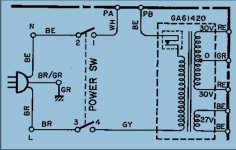
Finally the PNP boards have arrived. I am keen to test tonight while my friend is over for a second opinion. However, I only have a 30v transformer – could it fry the transistors even if I play for 30 mins or so at low volume?
The AC power input terminal has no markings on it so I don’t know what wires I am attaching to which screw…
And here is a diagram of the transformer I am using attached below
Can I use the 27V secondaries in the diagram?
I am used to SMPS and basic class D modules, so excuse my ignorance
And here is a diagram of the transformer I am using attached below
Can I use the 27V secondaries in the diagram?
I am used to SMPS and basic class D modules, so excuse my ignorance
Attachments
Playing at low power is the worst possible state for a Class A amp. The more power you pump into the load, the less is dissipated by the amp.
A 27 volt transformer (make sure it is rated sufficiently) will give over 35 volts DC under heavy current draw as here. That is OK as long as:
a/ your heatsinking is sufficient.
b/ you are sensible with the bias current. If you only want to play at low volume then adjust R2 (original component references) to give a lower current.
The AC power input terminal has no markings on it so I don’t know what wires I am attaching to which screw…
And here is a diagram of the transformer I am using attached below
Can I use the 27V secondaries in the diagram?
I am used to SMPS and basic class D modules, so excuse my ignorance
Re adequately rated can you post a photo with some reference to size - like a ruler. If you have accurate kitchen scales you could also weigh it.
I suspect the 27 volt winding serves a low power auxilliary purpose to the other winding pair - the diagram looks old.
One thing you could do is measure the resistance in each winding. It the 27 volt one measures the highest it will be a no goer.
It mentions 350VA and 400W (for Australia), so it's likely that you have >300VA
The centre tapped secondary is 300VA/60Vac = ~5Aac
You can't take a full VA from just one half of the centre tapped winding.
Can you access the centre tap?
Is it possible to separate the two wires that form the centre tap?
If so, then you can separate and parallel the two half windings. This way you get the full VA for the paralleled winding.
I would not use this transformer as a permanent installation.
However for a temporary test the centre tap can be a ground with the positive tab of the supply cap connecting to this - with each 30 volt a.c. winding connected to the positive (banded end) of a rectifier diode with the opposite diode ends joined at the capacitor negative tab. (I am assuming a negative rail set up)
You would need a suitable value resistor to reduce the current draw and the appropriate to reduce the voltage of the supply - this in series with the individual module under test.
The two diode rectifier scheme reduces the supply efficiency by 50 %. Don't try running two modules at the same time.
Last edited:
- Home
- Amplifiers
- Solid State
- JLH 10 Watt class A amplifier