Hi all
It is interesting that the JLH10-watt is still discussed some 45 years later. While there is much discussion on the accuracy of simulator tools, at least these may be used to provide greater insight than previously possible. In view of this I attempted to investigate the "three-mod" frequency solution with some surprising results.
First, as originally configured, the bandwidth is around 2MHz and the unity gain is around 10MHz (using BC307B input-BD139 driver and 2N3715 output devices as I had models for these). This implies a faster than 6dB slope with potential instability but the (simple) phase margin appears to be 40 degrees, so at face value it is stable, but not unconditionally.
With the three-mod compensation, it appears each has a detrimental effect. The output RC stage doubles the load, reducing the unity gain frequency point to 5MHz. The 1nF feedback capacitor rolls off the gain at around 60kHz which may limit the perceived "openness" due to composite frequency roll-off (20kHz hearing plus 60kHz amplifier could be only 15kHz net); and finally the RC network across the driver base reduces the gain from about 100kHz upwards, but this would have little impact, I would think, on the audio performance.
On the other hand a simple capacitor compensation or RC network between the driver transistor collector and emitter of the input transistor can improve the phase margin. Without going further into this, a capacitor of around 330pF would limit the frequency response to 200kHz (ten time the audio band) but because this cannot reduce the gain to below 1 the RC network across the base of the driver is still needed. With 100 ohm and 1nF for the driver base network a 330pF and 220 ohm compensation capacitor appears to give a phase margin of 90 degrees.
I would suggest that if capacitive loading were a problem then the better solution would be to use an LR output network and then couple this with the RC shunt network to avoid excessive loading.
Dear Ellis,
A small set of figures will help me immensely.
--gannaji
Hi all
It is interesting that the JLH10-watt is still discussed some 45 years later. While there is much discussion on the accuracy of simulator tools, at least these may be used to provide greater insight than previously possible. In view of this I attempted to investigate the "three-mod" frequency solution with some surprising results.
First, as originally configured, the bandwidth is around 2MHz and the unity gain is around 10MHz (using BC307B input-BD139 driver and 2N3715 output devices as I had models for these). This implies a faster than 6dB slope with potential instability but the (simple) phase margin appears to be 40 degrees, so at face value it is stable, but not unconditionally.
With the three-mod compensation, it appears each has a detrimental effect.
On the other hand a simple capacitor compensation or RC network between the driver transistor collector and emitter of the input transistor can improve the phase margin. Without going further into this, a capacitor of around 330pF would limit the frequency response to 200kHz (ten time the audio band) but because this cannot reduce the gain to below 1 the RC network across the base of the driver is still needed. With 100 ohm and 1nF for the driver base network a 330pF and 220 ohm compensation capacitor appears to give a phase margin of 90 degrees.
I would suggest that if capacitive loading were a problem then the better solution would be to use an LR output network and then couple this with the RC shunt network to avoid excessive loading.
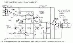
A point I forgot to make earlier is the need for an output zobel 8R and 100n as per the ClassAB circuit (Wireless World -June and July 1970).
You mention a 330 pF capacitor is not able to reduce the gain below 1. This connected around an inverting amplifier stage involving the second transistor with a capacitor in the feedback loop.
The capacitor impedance would reduce tending to zero with increasing frequency, thus for the stage gain to be 1 the impedance values of the base input to the transistor and for the feedback loop would have to be equal. That might arise at some frequency point but not if the bar is lifted high enough. My thinking was for 30 MHz fT output devices.
I wonder if you have looked at this in a different way.
A point I forgot to make earlier is the need for an output zobel 8R and 100n as per the ClassAB circuit (Wireless World -June and July 1970).
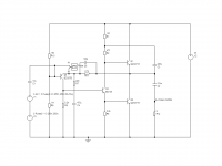
Is this the drawing referred ?
Attachments
Hi batteryman. Interesting, thank you. Is there a difference here between class-A and class-B? JLH revised the '69 version of the 10watt amp in the following year (1970) with a simplified PSU....i.e. no semiconductors. I think he only noted a slight increase in low frequency distortion. Later he advocated regulated PSU's for his bigger class-B MOSFet power amps and spoke of better bass and channel separation as I recall. Given that the current drawn by the class-A will be much less variable than the average Class-B amp have you experimented with different PSUs on different classes?
Sorry to expect you to have done all the work.....
Merry Christmas and a happy New Year to all the JLH class-A crew.
Cheers, Jonathan
I haven't done any experiments with class A/B amps but when I get time I will build a passive psu for the high power JLH amp which I did try with a lab switch mode psu. (I'm using pairs of MJ15003 output transistors and have no stability issues)
I believe the answer for a passive psu is to massively over specify it which means big bulk and cost and requires a separate housing for it.
I remember using 600va of toroidal transformers some years ago, + several Coke can size reservoir capacitors, which dimmed the lights when switched on.
Is this the drawing referred ?
Yes. The driver stage is unusual in using a single device assisted by a boostrap for the PNP output. If you found this on Rod Elliots site there should be copies of the articles and some coverage of difficulties with ClassB transistor amplifiers.
I have a phrase for what you are describing.What is a power amplifier? Is it not a power supply modulator?
So in my view, not enough importance is attached to the quality of the power supply and in my experience, the best solution is to avoid at all costs, active devices in it, including capacitance multipliers.
The best results I have had with various diy amps over many years has always been with a generous transformer for each channel, with massive smoothing caps - 50,000uf or more. (I'd use many paralleled smaller caps to reduce the esr these days)
The downside is of course, the cost, but why build a state of the art amp and then skimp on the power supply?
Any active psu circuitry will impact its own signature on the sound, especially at high volume, and this can be compounded by speakers that are a difficult load.
A few years ago I built the high power version of the JLH amp and tried it with a laboratory switch mode psu - it did not sound that impressive.
Capacitance multipliers and regulated psus are tricks of the trade used to cut costs and keep down the size & weight of the amp.
"current capability".
To me the ability of the amplifier to meet the current demands of the reactive load is down to current capability.
The PSU must be part of the current capable system.
It is my belief that this assertion is wrong....................... Given that the current drawn by the class-A will be much less variable than the average Class-B amp ....................
The maximum supply rail current of a ClassA amplifier is equal to the output current to the load plus some small amount powering the amplifier.
The maximum supply rail current of a ClassAB amplifier is equal to the output current to the load plus some small amount powering the amplifier.
Essentially the peak rail current of both classes of amplifier are the same.
Now look at the minimum current in the supply rail.
In a ClassA amplifier the minimum current will drop to a tiny amount just to power the front end of the amplifier.
In a ClassAB amplifier the minimum current will drop to a tiny amount just to power the front end of the amplifier.
In both Classes of amplifier the minimums are near zero and essentially the same.
The difference between the minimum and maximum rail currents is essentially the same for both ClassA and ClassAB.
Where there is a difference is between how the rate of change varies as the rail current of ClassA increases from near zero compared to the ClassAB as it increases from near zero. Unless the ClassA amplifier has transistioned into ClassAB in which case the rate of change for both will once again be the same.
the temperature of the heatsink will depend on how the amplifier has been designed and built.I see, thanks
I was planning to use an old inkel ma420 as a case. the 2 x heatsinks measure about 170mm long 90 high and 40mm deep each
Will this be enough per channel?
All amplifiers are different.
You should have used a close rated fuse for the 600VA 230Vac transformer. It would be T2.5AI haven't done any experiments with class A/B amps but when I get time I will build a passive psu for the high power JLH amp which I did try with a lab switch mode psu. (I'm using pairs of MJ15003 output transistors and have no stability issues)
I believe the answer for a passive psu is to massively over specify it which means big bulk and cost and requires a separate housing for it.
I remember using 600va of toroidal transformers some years ago, + several Coke can size reservoir capacitors, which dimmed the lights when switched on.
To prevent the fuse blowing you should have used a soft start circuit.
The added resistance for this soft start would be 45ohms to 50ohms.
Then your lights would not dim.
there is no excuse for using a direct on line start of any transformer with a massively over-rated fuse that ends up dimming the lights.
BTW, dimming of the lights which are fed from a different fuse in your distribution board indicates that your mains source impedance was VERY HIGH. There may have been a fault in your mains or distribution board that required the attention of a qualified electrician to investigate and correct.
The dimming of a table lamp fed from the same socket as your transformer would indicate a high source impedance anywhere upstream of the wall socket. The fault could be in the house wiring rather than at the distribution board.
Last edited:
the temperature of the heatsink will depend on how the amplifier has been designed and built.
All amplifiers are different.
OK l will try it and do the finger test
OK l will try it and do the finger test
The figure given by Hood in the 1969 article for the dissipation of the output transistors is 17 watts each. He recommended finned heat-sinks 5 inches by 4 inches - the ones he used were anodized black.
For an example of the fin profile - this was similar to H0568 in Altronics catalogue. This example has a height of 55 m.m. Thermal resistance for these is 3.4 degrees C per watt - with a 57.8 degrees C increase over ambient probably quite high where you live in summer.
Looking at other heat-sinks in their catalogue the thermal dissipation does not improve in proportion to height. Looking at the Extra Heavy Duty flange types the dissipation of a 300 m.m. height (H0592) is only twice that of a 75 m.m. version (H0580).
The choice of heat-sink Silicon Chip magazine made for their Class A projects was two off the Diecast H0545 with a height of 75 m.m. and width 300 m.m. This has a thermal resistance of 0.37 degrees C per watt - with a pair of outputs per each heat-sink the temperature rise would be 13 degrees C over ambient. The transformer will generate some heat inside a case so this would need to provide adequate ventilation.
I think you will need larger heat-sinks and with these cannot see the bulk of the hardware being adaptable to the chassis you are planning to use.
You could do what Silicon Chip did in 1998 adapting a 2 unit high rack case by removing the side panels and substituting the heat-sinks.
They removed the power supply in a plastic instrument case connected by an umbilical cable. The power supply was a regulated type. The Williamson valve amplifier of 1947 also had a remote power supply.
I followed that example for my 1996 project - except I had a metal workshop cut material for me to make my own case. I had a suitable case available from some junked electronic equipment for the regulated power supply - I needed a larger heat-sink, transformer and capacitors than the Silicon Chip example.
The capacitor banks are 30,000 uF per supply rail.
In the end the rectified voltage under load was a bit high and I was uncomfortable about that being presented to the regulators which would increase their heat dissipation.
I noted there had been an occasional problem of transformer buzz in the later Silicon Chip Class A project - mains variability in Australia.
The cure was to fit suppression chokes between the rectifier and the capacitor banks to lower magnitude of charging spikes by just enough. I incorporated these in my 1996 amplifier sometime in 2015 and it had the desired effect of reducing the voltage presented to the regulators.
Having lived with the change a while now there has been some unexpected improvement in the sound. The remote supply removes vibration and the transformer field away from the main chassis - I think of this as having benefits with the sound.
On dual supply rails I don't have any plans - I have the means since due to a problem in the post and my transformer being a custom order I ended up with two of them.
As many transformers are made with dual secondaries prospective builders could make use of this for separate supplies for each channel with the 1969 amplifier.
As to v.a. rating I had transformer failures with EI types when I built mine - the first 80 v.a. following the table in Hood's article - the second a 150 v.a.
Both Silicon Chip projects have used 160 v.a. rated toroidal transformers and no problems appear to have arisen with failures - which makes me doubt the quality of the EI ones I used.
All the same I don't see anything wrong with going to 300 v.a. toroid with a dual secondary winding.
Hi all
Further simulations suggest that, as I had expected, a simple phase-compensation capacitor should provide a greater margin without the need for the base-to-ground RC network as mentioned in my earlier post.
Regarding the unity gain issue, a capacitor connected to the emitter of the input transistor leads to an effective emitter follower with unity gain at high frequencies. I should have added "until the rest of the circuit causes further fall-off". This means if you want to use the three-stage compensation suggested by Linsley Hood the additional roll-off capacitor on the base of the driver it will in principle reduce the gain earlier - but delays the phase unless a resistor limits the phase shift at higher frequencies.
I therefore suggest that a simple compensation capacitor could be used to limit the frequency response as shown in the attachment - if constructors need this.
Regarding the use of 30MHz output transistors they offer a lower distortion (better gain linearity) but as posted several entries ago I found that a 33pF capacitor was essential to stabilise the unit.
Attachments
Hi all
Further simulations suggest that, as I had expected, a simple phase-compensation capacitor should provide a greater margin without the need for the base-to-ground RC network as mentioned in my earlier post.
Regarding the unity gain issue, a capacitor connected to the emitter of the input transistor leads to an effective emitter follower with unity gain at high frequencies. I should have added "until the rest of the circuit causes further fall-off". This means if you want to use the three-stage compensation suggested by Linsley Hood the additional roll-off capacitor on the base of the driver it will in principle reduce the gain earlier - but delays the phase unless a resistor limits the phase shift at higher frequencies.
I therefore suggest that a simple compensation capacitor could be used to limit the frequency response as shown in the attachment - if constructors need this.
Regarding the use of 30MHz output transistors they offer a lower distortion (better gain linearity) but as posted several entries ago I found that a 33pF capacitor was essential to stabilise the unit.
It is easy to get hooked on a single idea to enhance Hood's design by substituting the outputs for 30MHz power transistors. This has not come without some baggage.
I am suggesting a return to the basic design and try MJL21194 which is a nominal 4 MHz device - For data on this (and complement) see http://www.onsemi.com/pub_link/Collateral/MJL21193-D.PDF - SPICE models are available.
With unmatched devices it is claimed these complementary pairs have an open loop distortion figure of 0.8 % reduced to 0.08 % if pairs are matched. The 0.8 % holds up to 5kHz increasing to 0.95 % at 20 kHz.
I expect matching between NPN pairs ought to be better than between NPN and PNP complements and there are potential gains to be realised - since if an amplifier can be made more linear without feedback there is no need to push the envelope as hard in terms of frequency bandwidth.
Selecting Q3 for the highest gain is another consideration that impacts on distortion so there is scope to survey the field to see if there are better options. The BD139's I tested had less gain than 2N1711's. Some Motorola BC639's were better still - I still have 2N1711's with their metal cans. One could glue an aluminium tab to a BC639.
For completeness Hood subjected his amplifier designs to testing with an 8 R test resistor with parallel capacitors of various values with a 10 kHz square wave input signal.
I dislike the idea of the 100 pF capacitor in the feedback loop - at high frequency it will be a low impedance path for any intrusive signals to reach the inverting input.
If you run the simulation with the load mentioned I suspect you may find the need for an output zobel network and possibly an output coil to mitigate the risk.
One reason for wanting to use modern high performance output transistors is that their gain is generally higher and their gain linearity better than the older types, and the higher fT is almost a burden.
My comments were addressing only the recommendation that JLH made regarding "three changes that had to be all together or none". The feedback capacitor improves phase margin, but I agree in a real amplifier a small inductor would be needed or would be useful in the output to suppress HF pickup as mjona says. In adding an L(R) component an RC component restores the resistive loading at high frequencies and although many people call this Zobel it might not be in the strict sense that a Zobel is supposed to offer a uniform impedance (i.e. the L and C impedances should provide a uniform loading) but may not in an amplifier output network.
The MJ21194 device is a good transistor and has a flat gain characteristic but is on the low side. Looking back at the data sheet for the MJ481 transistor it has a spec. gain of 30-200 at 1A. JLH used devices with gains from 40-160 or thereabouts. However, the gain fall off at high currents is significant (as it was for many 1970-era devices) and could be as low as 10 at 3A. This was the reason that the original amplifier needed a standing current of around 1.2A rather than the theoretical 900mA that was debated at the time. The standing current has to be set by half the base current needed for peak output, (plus a bit) as one transistor's current has to come from the other in JLH's simple design.
Using modern transistors would largely eliminate the open loop non-linearity due to high current roll-off. The MJL3281A for example has a minimum gain of 75 at 1 and 3A, and would potentially enable the standing current to be reduced.
Regarding the BD139 I agree that older devices may have a lower gain than the 2N1711. Originally these were spec'd at 40 min. at 150mA and 25 at lower and higher currents. However, recent specifications now show 63 min. gain on some manufacturer's datasheets. There is also an option of specifying the -16 gain group which has a minimum gain of 100, or maybe some can find old stock 2N3019. The JLH original needs as much gain as it can get so the higher the better.
One other point to bear in mind is that the MJ21194 is a big chip. It is probably four times the size of the MJ481 device and has a higher capacitance in the junctions, although it has to be said that so do the MJL3281A's. Larger capacitances need more drive to maintain a frequency response. Of course the MJ481 is obsolete, and my recommendation is to use MJL3281A's or similar (2SC5200 etc) in new build JLH "originals".
I had no problem using 33pF stabilising capacitors without an inductor on real speakers, but it would be safe to include the output inductor.
It is interesting to have this discussion since it gives people more freedom in choice and judgment to achieve whatever result they are seeking.
I see in other discussions some evidence showing that BD139 is a quality device in terms of Early Effect.
The MJ or MJL21194 devices have fT specification of 8MHz at a current of 1A. With these the outputs will be working in that region.
The correspondence you looked at re the three element modifications, I see the amplifier (using MJ481's) is capable of a good square wave at 1MHz the limit of the generator used, that the voltage gain -3dB point using better equipment was above 1.5MHz although power output falls beyond 200 kHz. I see no lack of speed or speed wobbles.
The dominant pole for stability is set by the output stage rather than the voltage gain- phase split transistor. The preceding transistors had higher fT specifications - an amalgam of variable parameters that take capacitance into account.
With a constant current Class A stage capacitance is not going to vary greatly - so it can be used to set the dominant pole by selection of a device having a lower fT than the transistors that precede it.
Hood made this point in the book on Valve and Transistor Audio Amplifiers published in 1997 - pretty much his last word on this amplifier.
The amplifier has been built with MJ15004 which has 1000 pF Cob compared with 200 pF for the obsolete MJ481.
There is some informative discussion here http://www.diyaudio.com/forums/soli...tor-families-audio-power-output-stages-3.html
One point not mentioned so far is that increasing the closed loop gain can benefit the stability of an amplifier.
With a closed loop value of 13, I have to use a line amplifier to boost the signal to the input.
One way to boost the gain of a voltage amplifier is to increase the current it draws. Higher current gain of the output stage transistors will help too but there might be a balance that allows the closed loop to be tweaked without sacrificing audio performance.
This might be useful with implementing MJL3281's. I have some however I am not planning to use them in this design.
I have been enjoying my chineese JLH69 for a good month now, and still love its "presence", especially in the lows. However, in high mids and highs, I would like it a bit more pronounced. Will swapping the 2n3055 for other devices change this? In search of the answer, I tried going through this thread "cover to cover", but around page 50, found out my electronics knowledge sucks and I better just ask the question... What is the easiest and least scientific mod for this great amp?
I planned to swap the 2955 in my Chinese pnp jlh amp with 15034. I've received them but the not done the swapping yet. However I did swap the input cap with a solen cap and paralleled a 10uf solen with the output cap. That made an improvement on the mids and top
Sent from my iPhone using Tapatalk
Sent from my iPhone using Tapatalk
Hi Peroz,
I used the MJ15003 and it sound great for my taste.
Have a look here for Output transistors; The Class-A Amplifier Site - JLH Class-A Update
This is what I'm refering to;
''Output transistors.
The 2N3055s were replaced with MJ21194. In comparison with these the 2N3055s sound grey and rather diffused with less sense of authority, less detail and a more prominent treble quality. In contrast, the MJ21194s have a noticeably firmer sound with more ambience in the treble and greater detail. More natural generally. Reluctantly, they were removed from the circuit due to a faint hum which was not present with the 2N3055s.
Wanting to try something else, and now with the strong impression that the 2N3055s were less than ideal, I tried some MJ15003s.
This time, a substantial improvement over the 2N3055s. The MJ15003's bass is both tauter and more authoritative, with cleaner treble and greater textural detail.''
p.s. The above is for the bipolar JLH version, for my JH 1969 I used the ON semi NJW21194.
BR,
Eric
Last edited:
Sorry , I meant MJ15004 pnp not 15034. In my diy jlh 96 I also used the MJ15003 with great improvements over 3055 [emoji4]
Sent from my iPhone using Tapatalk
Sent from my iPhone using Tapatalk
Sorry , I meant MJ15004 pnp not 15034. In my diy jlh 96 I also used the MJ15003 with great improvements over 3055 [emoji4]
Sent from my iPhone using Tapatalk
Easy to get mixed up if someone builds a PNP output version. I did that in my last post quoting MJ15004 instead of MJ15003.
- Home
- Amplifiers
- Solid State
- JLH 10 Watt class A amplifier