hi
UJ3N065080K3S model is already in FULL_JFET.txt, but i don't know if it's a good idea to use a mosfet in the diagram
but i donc know how to create a Jfet subckt
yes R6 need to be adjusted but the quiescent current is not a problem.
In simulation the gain is too high, my 2sj103 model should be wrong
UJ3N065080K3S model is already in FULL_JFET.txt, but i don't know if it's a good idea to use a mosfet in the diagram
but i donc know how to create a Jfet subckt
yes R6 need to be adjusted but the quiescent current is not a problem.
In simulation the gain is too high, my 2sj103 model should be wrong
Last edited:
Hi!
In the next thread there are 2sj103 models (JFET and MOSFET SPICE models). It seems that this is the only 2sj103 model that can be found.
.model 2SJ103Y PJF(beta=1.053m vto=-1.342 is=1n cgd=8.0445p cgs=4.9555p lambda=34.8 mfg=TOSHIBA)
.model 2SJ103GR PJF(beta=2.283m vto=-1.342 is=1n cgd=8.0445p cgs=4.9555p lambda=16 mfg=TOSHIBA)
.model 2SJ103BL PJF(beta=5.092m vto=-1.342 is=1n cgd=8.0445p cgs=4.9555p lambda=7.2 mfg=TOSHIBA)
Last edited:
I also found such models:
.MODEL 2SJ103 PJF(BETA=2.197M RS=76.76 RD=76.76 BETATCE=-.5 LAMBDA=735.3U VTO=-2.037 VTOTC=-2.5M CGD=18.95P M=.5045 PB=.3905 FC=.5 CGS=17.02P ISR=38.48F NR=2 IS=3.848F N=1 XTI=3 ALPHA=10U VK=100 KF=1E-18 AF=1)
.MODEL 2SJ103BL PJF (BETA=898.438U IS=10F RD=200 CGD=11.9398P CGS=14.4P)
.MODEL 2SJ103GR PJF (VTO=-1.62622 BETA=16.1875M LAMBDA=1M IS=10F RS=186.826 CGD=13.2918P CGS=14.3694P PB=806.232M KF=0.001F AF=500M)
hi
...In simulation the gain is too high, my 2sj103 model should be wrong
Hi.
Well, when you can check the model with a ready-made device.
HI
With the difficulty of finding input jfets, I thought why not bipolar, so I tried to simulate this one
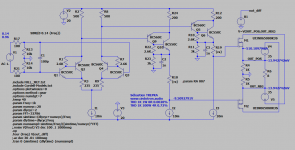
Jpatay, this is the amp so I spoke to you in December, but I just invert the schematic and put the Power Jfet that you proposed
Hi Seb!

It is very good that you have completed this circuit. It would be nice to collect and listen to it.
And also check for thermal stability. Spring. I don’t want to do anything.😉
It is not completed circuit, just a test and not thermal stable with general ccs.
I need to found a negative CCS
I need to found a negative CCS
I measured the output impedance of the amplifier by the method of two loads at different values of the quiescent current.
I = 100mA / Rout = 0.14R
I = 200mA / Rout = 0.12R
I = 300mA / Rout = 0.12R
I = 100mA / Rout = 0.14R
I = 200mA / Rout = 0.12R
I = 300mA / Rout = 0.12R
Last edited:
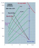
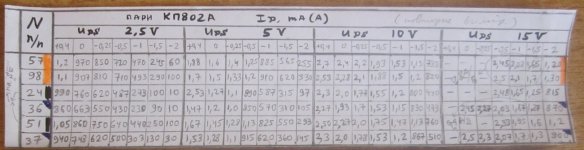
Measured its stock SIT-JFET KP802A (КП802А).
A total of 114 pieces, 87-92 production years.
Began to disassemble the "fours".
In the attachment is a table of those with the highest drain current initial, the tip of the iceberg.
Schedule for the "average" of the four transistor 57 / 98 - 36 / 37.
Average parameters calculated: Ri=(15-5)/(1,89-0,747)= 8,7 Ohm, S=(2,27-1,49)/(1,5-0,5)=0,78 A/V, u=RixS=6,8 units.
Output impedance of the common-drain amplifier:
1/S=1,28 Ohm.
It is seen that the output arm voltage should be kept 18-19 V. For these numbers.
Attachments
Last edited:
Could you use your native tongue?
You're welcome:
http://www.diyaudio.ru/forum/index.php?topic=6606.60
Hi do you think this amplifier could be used with lateral mosfet ?
I have 4 exicon ECW20N20-S
I have 4 exicon ECW20N20-S
Last edited:
Hi do you think this amplifier could be used with lateral mosfet ?
I have 4 exicon ECW20N20-S
Muscovites listened to the amplifier on 2SK1529, 2SK1530 and got a good result.
ECW20N20 excellent transistors
HI nice 🙂
so he start from this one :
https://www.diyaudio.com/forums/att...circlotrons-negative-feedback-_-1_303-104-jpg
so he start from this one :
https://www.diyaudio.com/forums/att...circlotrons-negative-feedback-_-1_303-104-jpg
Last edited:
in fact all my transistors are with my parents since I was preparing the sale of my house before the quarantine, so I cannot check what I have now
But I have the 4* ECW20N20-S and I know I have J113, 2SJ103Y, 2SK246Y, 2SK246GR
y could buy J112 or J111 from mouser
do you have the final values used by Alexey Semin ?
But I have the 4* ECW20N20-S and I know I have J113, 2SJ103Y, 2SK246Y, 2SK246GR
y could buy J112 or J111 from mouser
do you have the final values used by Alexey Semin ?
do you have the final values used by Alexey Semin ?
In the amplifier of Alexey: VT7-VT12 - J112.
VT5, VT6 - 2SJ103BL. VT1- VT4 - transistors of domestic production.
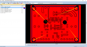
Not possible to order at PCBWay because of errors
Trying to order the board at PCBWay gives me an error from them: "Failed reason: Board outline is not clear"
The ZIP-file with the Gerbers are not possible to download, either. Problem seems to be that one layer has a square board, some other layer has rounded corners.
PCB manufacturing can be ordered here:
JFET-only Circlotrons without negative feedback. - Share Project - PCBWay
Trying to order the board at PCBWay gives me an error from them: "Failed reason: Board outline is not clear"
The ZIP-file with the Gerbers are not possible to download, either. Problem seems to be that one layer has a square board, some other layer has rounded corners.
Attachments
- Home
- Amplifiers
- Solid State
- JFET-only Circlotrons without negative feedback