Drawing a load line
I tried to understand how the attached very simple circuit of juma works and how can I draw a load line for it, but I'm not that bright 🙁
I can simulate it, modify it for higher gain or lower THD but I want to understand more.
I read this article Simulating a FET Amplifier, however, it calculated the Rs by knowing the Vgs and Id based on the load line readings.
Can somebody explain it to me. Thanks!
Attachments
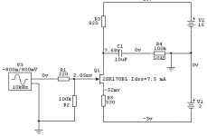
Hi,I tried to understand how the attached very simple circuit of juma works
that 7.68V reading tells you the voltage across the drain resistor.
It indicates that the sim has biased the jFET at ~120% of Idss.
You must reduce the bias current.
The -52mV confirms the bias current.
The -ve source voltage will become slightly +ve when the bias current is <Idss.
This will then be the Vgs and is normally a negative voltage.
The sim is showing a +ve Vgs voltage (the gate voltage is above the source voltage).
Last edited:
Hope juma don't mind that I'm using his drawings... thanks!
I found back in the thread another circuit of this kind, which is probably ok (attached).
Could you explain me this:
- Does the negative supply is needed to obtain a higher Id using a higher Rs? as if using Rs to ground (a much lower Rs would be needed in this case)
From juma's explanation from post #705 seems so and also to lower the gain.
- But then how to draw the load line for it?
- 2SK170 having the pinch off Vp around 0.45V, how come that it's working with a 2Vpp signal? I can see it in sim (hopefully next week try it), but don't understand why 😕
Thanks!
Attachments
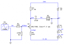
The sch. in post#841 contains an error - where it says "Idss=7.5mA" it should have said "Idss=10-12ma" and it might take a V grade k170 for that.
The sch. in the post #843 is ok
The sch. in the post #843 is ok
Hope juma don't mind that I'm using his drawings... thanks!
I found back in the thread another circuit of this kind, which is probably ok (attached).
Could you explain me this:
1. Does the negative supply is needed to obtain a higher Id using a higher Rs? as if using Rs to ground (a much lower Rs would be needed in this case)
From juma's explanation from post #705 seems so and also to lower the gain.
2. But then how to draw the load line for it?
3. 2SK170 having the pinch off Vp around 0.45V, how come that it's working with a 2Vpp signal? I can see it in sim (hopefully next week try it), but don't understand why 😕
Thanks!
1. Right
2. The same way as for any similar amplifying device. Google for it.
3. Study the transfer characteristics in the datasheet and think Vgs, not Vin to ground.
transformer
I have started the project!
What is the current draw of the circuit.
i intend on using 2 transformers with 0 18 V ac out . Will a 300ma current specification be enough for each channel ?
cheers
kp93300
the schematic is posted
I have started the project!
What is the current draw of the circuit.
i intend on using 2 transformers with 0 18 V ac out . Will a 300ma current specification be enough for each channel ?
cheers
kp93300
the current consumption is roughly Vcc/2 / 680r ~18mA. This assumes the output DC is set to half the supply voltage.
Let's assume two channels @ 20mAdc.
Total DC current supplied is 40mA.
The AC current rating of the transformer should be >=4 * DC current, i.e. >=160mAac.
A 300mAac transformer should run cool.
These tiny EI transformers have an enormous regulation. Your 18Vac transformer on zero loading could give near 33Vdc after the smoothing caps.
Last edited:
thanks Andrew for the reply.
Such tiny transformers are very cheap as my neighbour can wind it for me.
I will use 2 trans rated at 300 ma each.
kp93300
Such tiny transformers are very cheap as my neighbour can wind it for me.
I will use 2 trans rated at 300 ma each.
kp93300
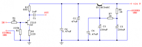
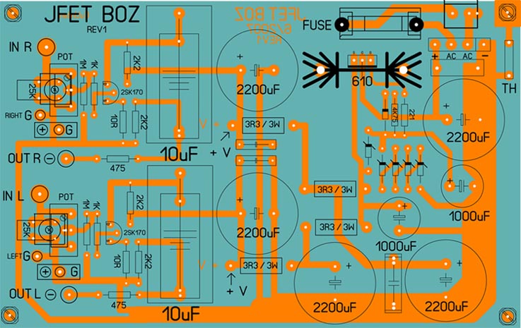
OK...I'm going to try a layout similar to Manu's as seen here:
I have 2 questions...
1. What would be the best way to wire up a center tapped xformer? Namely what to do with the center tap?
2. How would I wire up a toroid with dual secondaries? Namely, how to wire up the 4 secondary wires? Lets say its an Antek with one blue and one green per secondary.
I have 2 questions...
1. What would be the best way to wire up a center tapped xformer? Namely what to do with the center tap?
2. How would I wire up a toroid with dual secondaries? Namely, how to wire up the 4 secondary wires? Lets say its an Antek with one blue and one green per secondary.
go read
http://www.diyaudio.com/forums/diya...udio-component-grounding-interconnection.html
He tells you to connect the centre tap to the smoothing caps. Then to connect your PSU Zero Volts to the main Audio Ground. He tells you the options for locating that Audio Ground and none of them are in the PSU!!!!
http://www.diyaudio.com/forums/diya...udio-component-grounding-interconnection.html
He tells you to connect the centre tap to the smoothing caps. Then to connect your PSU Zero Volts to the main Audio Ground. He tells you the options for locating that Audio Ground and none of them are in the PSU!!!!
OK, I have the JFETBOZ up and running on the Dell PSU 19.5V. Running ERSE coupling caps, Dale CMF50 resistors, Nichicon electrolytics, an alps RK27 pot, and matched toshiba JFETs.
This has really brought the F5 to life. It surpasses any preamp that I have tried to date.
Thank you Nelson Pass and DIYAudio.
This has really brought the F5 to life. It surpasses any preamp that I have tried to date.
Thank you Nelson Pass and DIYAudio.
Manu is my Yoda 
don't be too critical in this case
even if Andrew is certainly right , in this case - with currents involved in Jfet BOZ operation - any way of grounds organizing isn't critical .
besides - I know that Manu later made some much better pcbs
don't be too critical in this case
even if Andrew is certainly right , in this case - with currents involved in Jfet BOZ operation - any way of grounds organizing isn't critical .
besides - I know that Manu later made some much better pcbs
Thanks Zen ...🙂
It should be clear for everybody that I made this PCB-layout simply in order to test the JFetboz at the time it was published. And it worked fine for my purpose. I never pretended the layout were perfect, nor ready for production of any kind.
Newly cjkpkg found some similar-looking PCBs for sale on the web and contacted me.
I told him that I don't have anything to do with that, but that he could have the PDFs of my silly layout, if he wants, in order to etch his own PCBs or adapt the layout to his needs...
Thats all ...
Thanks Andrew for the links.

Manu
It should be clear for everybody that I made this PCB-layout simply in order to test the JFetboz at the time it was published. And it worked fine for my purpose. I never pretended the layout were perfect, nor ready for production of any kind.
Newly cjkpkg found some similar-looking PCBs for sale on the web and contacted me.
I told him that I don't have anything to do with that, but that he could have the PDFs of my silly layout, if he wants, in order to etch his own PCBs or adapt the layout to his needs...
Thats all ...
Thanks Andrew for the links.
I wouldn't place even a small bet on it ...besides - I know that Manu later made some much better pcbs
Manu
I did try to do the toner transfer method of Manu's design I got less than desirable results. I found a pcb online that I was able to utilize into my end result.
I incorporated the necessary values as discussed early in this thread and used some matched JFETs that I acquired from BLUES. The PSU section is a relatively straightforward design that seems to be loosely based on what has been published for the original BOZ and what Manu came up with also early in this thread.
Thanks for the pointers everyone. This is a terrific amp that is very complementary to the F5.
This is a terrific amp that is very complementary to the F5.
I second that, mucho ! 🙂
Manu
This is a terrific amp that is very complementary to the F5
You really think so?
I'm thinking about making one for a friend. He's building the F5 first, but needs a preamp too. Thought I'd help him along...so I can get my 2 F5s back. 😉
yes,
I tried the F5 with the B1 Buffer and with the source I normally listen to there was not enough gain.
I started thinking about the original BOZ but the JFETBOZ just seemed a little easier on the parts list and I was able to utilize an extra Dell laptop adapter I had to further reduce the complexity. Plus I had a nice Hifi2000 small galaxy chassis that would not have worked if I had to build a PSU to supply the BOZ voltage.
The gain is bountiful and the sound is very nice.
I have a Dell 19v power supply leftover too, but want to try the 15v Radio Shack battery. RS also has a 15v wall-wort PS, but at $28, it's a bit pricey.
Thanks,
V~
Thanks,
V~
- Home
- Amplifiers
- Pass Labs
- Jfet BOZ