Exquisitely put, Valery!
Abetir, that is very interesting. The one you drive one end of two complementary CCSs to drive a 2EF is quite novel, I have not seen this before and I expect it would be very, very fast as effectively the VAS is grounded base. I noticed you have avoided lag compensation; this is innovative design. Yours, or someone elses? It's clever....... and the pcb is beautiful!
Hugh
Exquisitely put, Valery!
Abetir, that is very interesting. The one you drive one end of two complementary CCSs to drive a 2EF is quite novel, I have not seen this before and I expect it would be very, very fast as effectively the VAS is grounded base. I noticed you have avoided lag compensation; this is innovative design. Yours, or someone elses? It's clever....... and the pcb is beautiful!
Hugh
Hi Hugh,
It's actually mine 😉
You can see more details, as well as some live measurements in combination with my non-switching OPS here:
My Ampliwire front-end live test
This kind of current-driven VAS came out pretty cool - it's simple, fast, linear and very stable even with no lag (Miller) compensation at all.
Cheers,
Valery
Attachments
MosFETs don't have and "optimal" bias voltage. That applies to a ClassAB BJT output stage.
MosFETs crossover distortion becomes less as output bias is increased.
Youre saying nothing, crossing, paradoxally.
they are same as bjt, except for the voltages, Vts for MOSes and 0.7 for bjt.
even for darlington is 0.7.
Youre sayin MosFETs crossover distortion becomes less as output bias is increased.
This is that optimal bias voltage. ??
Exquisitely put, Valery!
Abetir, that is very interesting. The one you drive one end of two complementary CCSs to drive a 2EF is quite novel, I have not seen this before and I expect it would be very, very fast as effectively the VAS is grounded base. I noticed you have avoided lag compensation; this is innovative design. Yours, or someone elses? It's clever....... and the pcb is beautiful!
Hugh
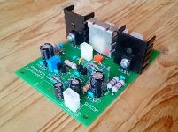
Thank you sir for the appreciation, the pcb lay-out was my work, the design concept was Valery's.
Best regards!
Albert
The heatsink on top seems to be a good candidate for use in this amp...Industrial grade taken from an smps. 😉
An externally hosted image should be here but it was not working when we last tested it.
The heatsink on top seems to be a good candidate for use in this amp...Industrial grade taken from an smps. 😉
An externally hosted image should be here but it was not working when we last tested it.
Those ones look very good 😎
MosFETs don't have and "optimal" bias voltage. That applies to a ClassAB BJT output stage.
MosFETs crossover distortion becomes less as output bias is increased.
The application note says optimum bias is around 100 m.a. page 3 discusses this point. The thermal coefficient is said to zero at that crossover level from positive to negative.
While such a level is ideal for class ab design, on the negative temperature coefficient part of the graph, a double device should be able to work in class a at twice the 500 m.a.you quoted as the yardstick given by Borbely. These devices cost roughly half that of the Hitachi original 2sk and 2sj replacements and the dual 16 amp device makes for a more tidy component layout.
Heatsink requirements for power dissipation is discussed in the application note along with other know how material.
Semelab make decent bjt devices but Mosfets cost more to make so there has to be a market for an upgraded range for audio use. Information in application notes can provide clues as to behind the scenes development going on. This one has opened my mind on prospective uses.
Valery,
I am working on the final retouch of the PCB lay out, will it be OK to include the gate protection diodes?
I am working on the final retouch of the PCB lay out, will it be OK to include the gate protection diodes?
The heatsink on top seems to be a good candidate for use in this amp...Industrial grade taken from an smps. 😉
An externally hosted image should be here but it was not working when we last tested it.
woow 😱
Valery,
I am working on the final retouch of the PCB lay out, will it be OK to include the gate protection diodes?
The best place to add them - bases of the drivers. Zener + diode, looking at each other (cathode to cathode or anode to anode).
ok, but if it stretches the pcb far larger than the violet lay out, It's a no go.
Yes, no real value from them in such a topology, so you can actually drop them - leave it "as-is".
Done! 🙂
PDF for home etching, by default printer paper size is A4.PCB size is 88x91mm (approx 3x4").
I have included options to use the commonly used rectangular white wirewounds for ballast
resistor, vertical mount. Also option to use Bourns multiturn type for the trimmer adjust.
Gate protection diodes are also included.
Cheers! 🙂
PS. Lenten Season is fast approaching here in my place, so no DIY for me in the next two weeks.
Attachments

The looks....😉
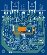
Hi Albert,
Great job! The only final refinement I would do - set the coil leads off the center (diagonal - start top left, end bottom right). This will give some space to make the trace between the 0R22 source resistors wider (as wide as possible - this is a high-currents area).
Cheers,
Valery
Ok, yet the part with the thinner tracks may look frail, one can only solder a heavy fill of lead into the traces, smps style. 🙂
Filling all the traces with a few leads does help in sealing the copper from corrosion. 😉
I will do a rework when it's possible, uploads in my network is painstakingly slow again
Filling all the traces with a few leads does help in sealing the copper from corrosion. 😉
I will do a rework when it's possible, uploads in my network is painstakingly slow again
.Looks good, come on lets see it with the heatsink 😀
mosfet54 burn in the mosfet 😉 give it a go...🙂🙄
you are very much welcome. 🙂
This would be my last DIY amp build, so my build is a slow one still lots of things to do. Now where is the fastest DIYer in the planet? ....still4? 😉 😀
- Home
- Amplifiers
- Solid State
- IRFP240/9240 Amplifier (simulated on TINA)