The looks again....😀
Excellent - exactly what I meant

But the archive in the previous post contains the previous version 😉
It's optimal in terms of the compromise between the dissipation/temperature and distortion level. As you can see from my measurements, at 80mA per pair distortion is already rather low. It doesn't make sense to run the MOSFETs hotter in order to decrease distortion further on. Distortion will go down a little bit, while the temperature will rise significantly. However, distortion is already low enough. This is true for high global loop gain designs.
just wondering, what is your ambient temperature when you do the testing?
it must be very cold in russia most of the year, i have worked there for six years in the sakhalin islands...
over here in manila, ambients of 30*C and more is common during these times...
Gate protection diodes are also included.
protection diodes in the pcb are actually connected at the bases of each drivers. 🙂
just wondering, what is your ambient temperature when you do the testing?
it must be very cold in russia most of the year, i have worked there for six years in the sakhalin islands...
over here in manila, ambients of 30*C and more is common during these times...
Well, the outside temperature varies a lot - from +30C in summer to -30C in winter, but the temperature in the apartment (where the amp is) is rather stable at +23...+25C.
Sakhalin islands are some 6 329 kilometers from me 😱
https://www.google.com/webhp?source...ewwindow=1&q=Distance+from+Moscow+to+Sakhalin
Hi Guys,
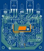
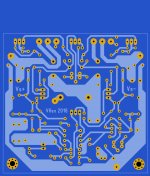
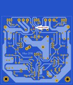
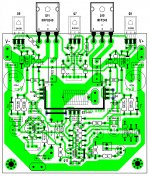
Abetir asked me about building his design so I etched a pair of boards and populated them. It wasn't working so I went over the layout and found some errors. It still isn't working so I'm thinking I am still missing something. Can you guys take a look and see if there is still something else I don't see. I'm posting the original layout along with the corrections I have made.
Thanks, Terry
Attachments
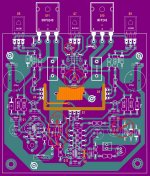
One thing I didn't mention is that I used MPSA18 for Q6/12. However I did use those in my Ampwire IPS and they work flawlessly. All I can think is that I still have something wrong. I'm hopeful one of you with fresh eyes can see what I have wrong.
Thanks again, Terry
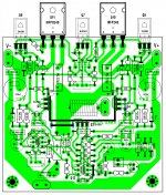
EDIT; I noticed that I was missing a couple of connections on the pic above that are not missing on the amp. They are at the base of Q12. I have corrected them on this pic.
Thanks again, Terry
EDIT; I noticed that I was missing a couple of connections on the pic above that are not missing on the amp. They are at the base of Q12. I have corrected them on this pic.
Attachments
Last edited:
I did not actually check the layout in terms of correc connections - only reviewed the trace width.
Albert, is it possible to check the layour automatically?
I use Diptrace and it's very easy there.
Albert, is it possible to check the layour automatically?
I use Diptrace and it's very easy there.
Sprint has a continuity test but it only lights up the connected traces. I have been all morning with a highlighter and the schematic checking for errors but haven't found any more errors. If there aren't any them it is possible I have a solder bridge that I have missed but I didn't want to chase ghosts that aren't there.
Terry, you are great! thank you.
I have also here my boards etched and ready to be populated and the heatsink is on standby.
I actually re-simulated the original schematic in TINA, because I could not make the VBE Led to light up, and output idle current is way too low. (supposed to be 75-100ma) even full wiper adjustment is done.
Don't exactly know why.
Valery, attached here is my re work of the schematic some values are adjusted (to avoid the precision types e.g. 3.6k, 240r, 510r. I currently don't have these types).
Cheers!
Attachments

Also I simulated, the schematic in Mikro-Cap to see the "on condition" of the devices. Say's VBE bias generator is in off state.
PS Today is the last day of Holy Week observance in my place. I will continue with my work this following week.
PS Today is the last day of Holy Week observance in my place. I will continue with my work this following week.
I have one channel working. On your latest drawing you changed the values around the VBE multiplier. I used the values from Valery's schematic. I had to change the trimmer to 200R and even that is a little too small. With it maxed out, I still have 48mV across the pair of 0.22R emitter resistors which is 102mA bias. Probably alright but I like to have a little wiggle room. Maybe the 1k8 or the 510 can me adjusted to make the 100R trimmer work. I did play some sine and square waves through it and they look very good. I'll wait until I have both channels working before I play any music through it.
Blessings, Terry
Blessings, Terry
^that is good news Terry, do not use my bias circuit values above, it cannot be trusted yet, if one resistor there gets shorted it could blow the rail fuses. I'm just playing with some values there. I was too late to realize that I named the schematic with a "final" extension. (my bad).
Cheers!
Cheers!
^i will change the 4.7k R18 to 5.6 or even 6.2k....
it is normal to change values to suit actual operating conditions,
it is normal to change values to suit actual operating conditions,
I have one channel working. On your latest drawing you changed the values around the VBE multiplier. I used the values from Valery's schematic. I had to change the trimmer to 200R and even that is a little too small. With it maxed out, I still have 48mV across the pair of 0.22R emitter resistors which is 102mA bias. Probably alright but I like to have a little wiggle room. Maybe the 1k8 or the 510 can me adjusted to make the 100R trimmer work. I did play some sine and square waves through it and they look very good. I'll wait until I have both channels working before I play any music through it.
Blessings, Terry
Terry, if you'd like to move the range of quiescent current to the lower values, you can increase 510R. 620R will be just about right, I think.
The higher overall resistors' value below the spreader's base - the lower the outputs' quiescent current is.
- Home
- Amplifiers
- Solid State
- IRFP240/9240 Amplifier (simulated on TINA)