Hi mjona,
Not much of a difference when comparing simulated results between #56 schematic and Valery"s #51 schematic but it seems #51 displays a higher THD at full power and I figure the resulting squarewave #56 has a slight edge.
Do you think #57 clipping behaviour has to do with its VAS loading? Its operating point though is a little off center, + rail clips earlier than - minus rail.
Best regards,
Albert
Hi mjona,
I figure the resulting squarewave #56 has a slight edge.
Best regards,
Albert
sorry, let me be clear what I meant with this. Referring to both #51 & #56 squarewave response at 20Khz full power, #51 displays a slightly wider gap in alignment with the desired squarewave output. My understanding then was, #56 slews much higher than #51. If my basic math is valid then,
SR= I/Cdom
where I is input collector current and Cdom is VAS miller cap. I am aware that other factor is involved here, but obviously #56 had a much higher collector current and a lower Cdom value.
An externally hosted image should be here but it was not working when we last tested it.
I would not worry at all about the shape seen on a 'scope with a 20 kHz square wave input as there is a trade off between stability and attaining perfectly square wave forms. 20 kHz is twice the normal test frequency and to reproduce this the rise time must be instantaneous. Frequency response is a function of rise time - the shorter this is the higher the frequency response would be - well beyond 20 kHz.
The download for your image does not complete so I am not able to see the differences between the three circuits.
Designers and builders can have their own preferences about circuit blocks and semi-conductor components they put in a design. Some people like differential VAS with current mirror loads. I prefer a common emitter amplifier with a constant current load as in Valery's Blameless model in post 51. Possibly he is of like mind - you have not heard from him on your modified circuit. You may need a new mentor for the differential VAS development you have in mind - I would be perfectly happy with the Blameless.
The download for your image does not complete so I am not able to see the differences between the three circuits.
- I would be perfectly happy with the Blameless
.
The image is just a representation of slew rate measurement. I am with the Blameless type as far as circuit simplicity is concerned, I have actually keep its basic nature with schematic #56, just added afew passive components there.
The cascaded VAS though may look more complex than the Blameless type, I do think it won't hurt if the added complexity will be worth the benefit that I can get.🙂
The discussion in this thread, is very informative.
http://www.diyaudio.com/forums/solid-state/168475-what-pros-cons-those-3-vas.html
@Valery, nice to hear from you.
Cheers!
Albert
We will see what Valery has to say about your Vas and current mirror loading. If you wanted to investigate the use of this form of loading it would have been simpler to adopt that for your input LTP.
Just wondering about your substitution of an LED for the 68 ohm resistor in the emitter connection of his Vbe stage. The resistor provides negative feedback in the process of dropping voltage making the structure more linear.
The 1 microfarad bypass capacitor was adequate with the resistor and I would have retained this.
If I understand it correctly from the works of Robert Cordell , the LED should be sufficient enough as a thermal sensor for a medium powered mosfet amplifier. I am liking it as a power indicator too.🙂
I've seen other circuits that also uses the resistor, notably the works of Anthony Holton, on the technical side I really can't tell which one is more effective. My understanding is that to make the VBE trannie more effective when driving mosfet outputs, a sensing agent has to be attached at its emitter.
I've seen other circuits that also uses the resistor, notably the works of Anthony Holton, on the technical side I really can't tell which one is more effective. My understanding is that to make the VBE trannie more effective when driving mosfet outputs, a sensing agent has to be attached at its emitter.
We will see what Valery has to say about your Vas and current mirror loading. If you wanted to investigate the use of this form of loading it would have been simpler to adopt that for your input LTP.
If you meant cascoding the input differential, I tried it and at lower frequencies it worked fine but at the higher frequencies in full power, THD hit 1% 🙁
If you meant cascoding the input differential, I tried it and at lower frequencies it worked fine but at the higher frequencies in full power, THD hit 1% 🙁
I meant loading the LTP outputs with a current mirror to increase the gain of that stage by combining the collector currents of each half.
This is one of the design strategies Self supports and has covered in his writings - except his focus was on input stages.
If I understand it correctly from the works of Robert Cordell , the LED should be sufficient enough as a thermal sensor for a medium powered mosfet amplifier. I am liking it as a power indicator too.🙂
I've seen other circuits that also uses the resistor, notably the works of Anthony Holton, on the technical side I really can't tell which one is more effective. My understanding is that to make the VBE trannie more effective when driving mosfet outputs, a sensing agent has to be attached at its emitter.
The base emitter junction of a transistor is sensitive to temperature. The best place for this is against the heat sink. Symbols can replace words and there is one next to the vbe transistor in Valery's circuit in post 51. I think you should stick with his scheme.
There are other independent ways to configure an on indicating light.
To continue on the thermal feedback theme there is a need for a solid foundation for a Vas so the Vbe transistor is not affected unduly by currents. The first question to be asked about options is whether a constant current arrangement or a current mirror is the better choice in that regard. I see concerns have been expressed about the effects heat has with HEXFETs hence my raising the question of the setting in the circuit structure as well as in the physical placement of the Vbe sense transistor.
My understanding is that by design principle there are trade offs, for example a high gain input may not need a current mirror. In simulation the push pull VAS exhibits instability when reducing the current to a low 10ma while the Blameless type goes fine from 7-10ma.
But let us wait for the more knowledgeable gurus to shed light on this matter.
BTW I 'm seeing the bias LED working in double purpose, that is why I mentioned power indicator 🙂
But let us wait for the more knowledgeable gurus to shed light on this matter.
BTW I 'm seeing the bias LED working in double purpose, that is why I mentioned power indicator 🙂
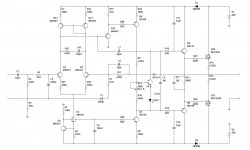
OK, here is what we can get if we add a current mirror and beta-enhanced VAS (EF in front of the VAS transistor). Note additional RC filter R27, C10 - helps to maintain stability with the lower value Miller capacitor.
This one is a gives a combination (always a compromise 😉) of low enough distortion, good slew rate and good enough stability.
Red LED at the emitter of the bias spreader actually reduces the thermal feedback sensitivity, which is good when you use the HexFETs at the output - the tracking curve comes closer to the gate current / temperature curve of the FETs. I have also slightly increased the gain up to 29db - just the standard one.
In terms of THD - it shows less than 0.002% at 1 KHz and less than 0.01% at 20KHz (50W @ 8 ohm). However, note more narrow stability margins on AC analysis graphs.
This is still very classic "Blameless" topology, described in detail in the book by Douglas Self, for example. There are still many areas for improvement - for example, the noise level (and distortion) can be lower, if you use better input transistors (like 2SC1845).
There are always the ways to improve performance by thinking about different topology approaches. For example, see this one here - very simple front-end, showing excellent performance:
AmpliWire VFA
Cheers,
Valery
Attachments

You beat me to it guru, I was about to post something about going into a full Blameless....well what can I say....
Hi Albert,
Want to try the real quality? 😀
Just looked at simulation of my AmpliWire VFA front-end with the OPS from your design we discussed. Very cool! This front-end is already live-tested with various OPS modules, showing excellent results. It's not only very low-distortion and rather high-speed - it's also very low-noise. Note - there's no Miller cap at all there - current-driven trans-impedance stage makes it possible.
Great performance/simplicity ratio 😎
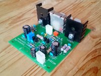
There is a PCB already developed for it down the link in my previous post (Idefixes did the layout) - you just have to add the OPS there.
Have fun 😉
Cheers,
Valery
P.S. Because of the open loop bandwidth wide enough, THD is below 0.001% at 1KHz and still below 0.006% at 20 KHz (50W @ 8 ohm).
If you increase the rails to +/-50V DC and add a 2-nd pair of the output devices, you will have a cool high-quality 100W @ 8 ohm amp.
Want to try the real quality? 😀
Just looked at simulation of my AmpliWire VFA front-end with the OPS from your design we discussed. Very cool! This front-end is already live-tested with various OPS modules, showing excellent results. It's not only very low-distortion and rather high-speed - it's also very low-noise. Note - there's no Miller cap at all there - current-driven trans-impedance stage makes it possible.
Great performance/simplicity ratio 😎
There is a PCB already developed for it down the link in my previous post (Idefixes did the layout) - you just have to add the OPS there.
Have fun 😉
Cheers,
Valery
P.S. Because of the open loop bandwidth wide enough, THD is below 0.001% at 1KHz and still below 0.006% at 20 KHz (50W @ 8 ohm).
If you increase the rails to +/-50V DC and add a 2-nd pair of the output devices, you will have a cool high-quality 100W @ 8 ohm amp.
Attachments


Last edited:

 for a few parts count! wonderful

Hi Albert,
Want to try the real quality? 😀
Just looked at simulation of my AmpliWire VFA front-end with the OPS from your design we discussed. Very cool! This front-end is already live-tested with various OPS modules, showing excellent results. It's not only very low-distortion and rather high-speed - it's also very low-noise. Note - there's no Miller cap at all there - current-driven trans-impedance stage makes it possible.
Great performance/simplicity ratio 😎
There is a PCB already developed for it down the link in my previous post (Idefixes did the layout) - you just have to add the OPS there.
Have fun 😉
Cheers,
Valery
P.S. Because of the open loop bandwidth wide enough, THD is below 0.001% at 1KHz and still below 0.006% at 20 KHz (50W @ 8 ohm).
If you increase the rails to +/-50V DC and add a 2-nd pair of the output devices, you will have a cool high-quality 100W @ 8 ohm amp.
What would your recommendations be in terms of output stage standing current and appropriate sized heat sinks for a single pair of devices.
Thanks for the tip about the LED. I had not thought the characteristics of this might be a match for a HEXFET gate diode at some operating level.
What would your recommendations be in terms of output stage standing current and appropriate sized heat sinks for a single pair of devices.
Thanks for the tip about the LED. I had not thought the characteristics of this might be a match for a HEXFET gate diode at some operating level.
Optimal standing current would be around 75mA per output pair. Size... One of my designs - Compact CFA - has got 2 pairs, mounted on a test heatsink 100x300mm (having not too many fins though) - when tested at continuous 50W for a long time (spectrums measurement, etc.), it becomes pretty hot. On the other hand, at the normal listening levels in the room, I rarely exceed 10W continuous power (although it's always good to have some extra power for possible peaks, as well as good current source/sink capability), so those heatsinks are just moderately warm. One of the HexFET advantages - they are rather powerful yet inexpensive.
- Home
- Amplifiers
- Solid State
- IRFP240/9240 Amplifier (simulated on TINA)