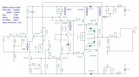
I have made D.White amp as per the schematic with single output.
It still sounds awesome and have no issues at all even running long hours.
Nice to hear that RSK

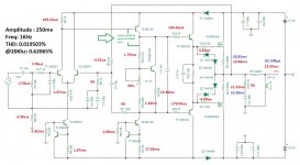
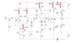
Ok, corrected RedFet schematic IRFP9240, source pin to nfb output, drain pin to psu rail. Attached also was the corrected David White mod, RedFet transient graph is at 20Khz freq 250mv amplitude. I will run more sim results by tomorrow, i'm probably straining my eyes now, looks like I'm missing things'....😱🙂
My friend visitor has just left and I did a quick check on my P3A before I handed it to him, one channel seems to be biased harder than the other channel. 🙂
Did I connect the P1 rotor at DWhites schematic the correct way ?
Thanks again,
Albert
Saying "P1 rotor position", I mean not the way it's connected (it's ok), but the resistance value it's set to (normally shown by percentage in simulators). Output transistors' quiescent current depends on that position and x-over distortion level strongly depends on quiescent current.
I think I had the DWhite mod running much better now adjusting the bias trimmer to 20% dc offset drops to -67mv. Output resistor R15 = 21.83mv R16 = -167.96mv.
...but looks like R16 is going over board, Ive been doing resistor values adjustment to R18 P1 & R21 (bias circuit) It does not show significant changes though...
...but looks like R16 is going over board, Ive been doing resistor values adjustment to R18 P1 & R21 (bias circuit) It does not show significant changes though...
Hello,
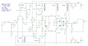
I got curious with the RedFet design..run it on simware with my usual driver stage addition..did some values adjustment/addition and voila!
I thought this one is a winner in terms of design simplicity and THD. I do however had to stop pursuing this project for a while as I need to exert more time with my other pending projects. I finally manage to finish two of my recent prototype amplifier, a Blameless TMC = many thanks to member Bimo for simulating it in LTSpice ) and the other was my take on IRSDAUDAmp1. I guess I had to do etching and soldering works for now.
I have attached the schematic zip file (in TINA simware) in case anyone happen to like it and do more analysis with it. I will however be checking the thread once in a while, hoping other member out there will finish what I have started, 🙂 my assumption is that the circuit has the potential to become a good sounding amp considering its simplicity. I thought the addition of LEDs is pretty cool but from the looks it didn't work out with positive results.
My thanks goes to you guys who pointed out my errors as I progress, special mention to member Valery who patiently guided me with my research.
Cheers!
Albert
I got curious with the RedFet design..run it on simware with my usual driver stage addition..did some values adjustment/addition and voila!
I thought this one is a winner in terms of design simplicity and THD. I do however had to stop pursuing this project for a while as I need to exert more time with my other pending projects. I finally manage to finish two of my recent prototype amplifier, a Blameless TMC = many thanks to member Bimo for simulating it in LTSpice
) and the other was my take on IRSDAUDAmp1. I guess I had to do etching and soldering works for now.I have attached the schematic zip file (in TINA simware) in case anyone happen to like it and do more analysis with it. I will however be checking the thread once in a while, hoping other member out there will finish what I have started, 🙂 my assumption is that the circuit has the potential to become a good sounding amp considering its simplicity. I thought the addition of LEDs is pretty cool but from the looks it didn't work out with positive results.
My thanks goes to you guys who pointed out my errors as I progress, special mention to member Valery who patiently guided me with my research.
Cheers!
Albert
Attachments
Why have you set T2 to operate at double the bias current of T1?
Why have you used the NFB (C3) to set the LF roll-off?
Why have you used the NFB (C3) to set the LF roll-off?
Why have you set T2 to operate at double the bias current of T1?
Why have you used the NFB (C3) to set the LF roll-off?
T2 is set as per the original RedFet schematic (or am I missing something?)
AC Transfer graph was set by default, starts at 1Hz should be set to start at 10Hz.
I would try removing R13 in the #44 post, R12 acts to balance the lower gm and higher Rds of the P-channel device
T2 is set as per the original RedFet schematic (or am I missing something?)
Yes, you're missing something 😉
For the best performance, collector currents of T1 and T2 must be equal - in this case LTP is balanced.
So if T3 collector current is 1.97mA, T1 collector current must be 1.97 / 2= 0.985mA. OK, 1mA will be fine.
Right now, collector currents: T1 - 0.655mA, T2 - 1.315mA.
LTP is disbalanced.
More details - a bit later.


Blameless! 😉
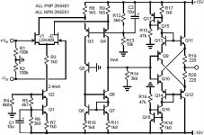
OK, here we go. Sorry - took some time... busy week 😛
This is a working circuit with very decent performance and enormous cost/performance ratio 😀
I tried to keep it as close to your original one as possible.
The devil is in the details. Key changes are:
1) Emitter degeneration (local feedback) in LTP (R21, R22) and VAS (R24) - improved linearity and local stability.
2) R3 value is changed in order to balance the LTP - now collector currents are equal.
3) R8 and R13 values are increased in order to keep the VAS and the drivers (accordingly) quiescent currents at reasonable levels.
4) Output FETs' quiescent current is set to roughly 100mA (setting the right value of R11 trim pot).
5) I have saved you one transistor in the VAS CCS - you can use the voltage reference from the LTP's one. Base stopper R20 helps to avoid possible artifacts. This change does not really influence performance - just cost optimization 😉
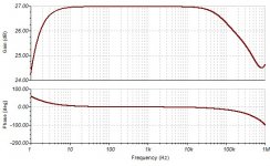
As a result - you can see the AC analysis attached:
Phase margin = 90 degrees;
Gain margin = 30db (a lot).
THD is below 0,05% at 1KHz and 0.09% at 20KHz (at 30W @ 8 ohm load).
Slew rate is relatively low - 17 V/uS - but still acceptable. If you want a higher one - you have to go for more advanced topologies.
All those numbers are simulation results. Live measurements may vary from them, however if the build is good - you'll see something pretty close.
Let me know if you have questions.
Cheers,
Valery
OK, here we go. Sorry - took some time... busy week 😛
This is a working circuit with very decent performance and enormous cost/performance ratio 😀
I tried to keep it as close to your original one as possible.
The devil is in the details. Key changes are:
1) Emitter degeneration (local feedback) in LTP (R21, R22) and VAS (R24) - improved linearity and local stability.
2) R3 value is changed in order to balance the LTP - now collector currents are equal.
3) R8 and R13 values are increased in order to keep the VAS and the drivers (accordingly) quiescent currents at reasonable levels.
4) Output FETs' quiescent current is set to roughly 100mA (setting the right value of R11 trim pot).
5) I have saved you one transistor in the VAS CCS - you can use the voltage reference from the LTP's one. Base stopper R20 helps to avoid possible artifacts. This change does not really influence performance - just cost optimization 😉
As a result - you can see the AC analysis attached:
Phase margin = 90 degrees;
Gain margin = 30db (a lot).
THD is below 0,05% at 1KHz and 0.09% at 20KHz (at 30W @ 8 ohm load).
Slew rate is relatively low - 17 V/uS - but still acceptable. If you want a higher one - you have to go for more advanced topologies.
All those numbers are simulation results. Live measurements may vary from them, however if the build is good - you'll see something pretty close.
Let me know if you have questions.
Cheers,
Valery
Attachments

Last edited:

OK I'm wide awake now, 
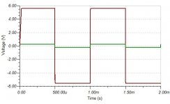
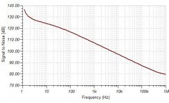
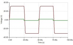
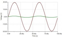
This modification done by guru Valery is impressive, the thing is a wide bander, at 20KHz the square edges is pretty intact and very visible. TINA Bode plot simulation shows a very stable, high gain amplifier that goes all the way in a straight line surpassing the 100KHz mark

TINA sim results:
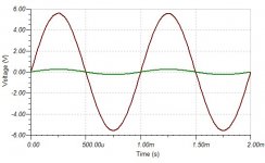
Amplitude = 250mv
THD 1KHz = 0.02%
20KHz = 0.04%
DC offset = -1.68mv
Given more free time I will design a PCB lay out for this amp, Valery's schematic.
Sorry, can't upload/post the graph Im using a smartphone, my 4G LTE Wifi router has become useless in my place
This modification done by guru Valery is impressive, the thing is a wide bander, at 20KHz the square edges is pretty intact and very visible. TINA Bode plot simulation shows a very stable, high gain amplifier that goes all the way in a straight line surpassing the 100KHz mark
TINA sim results:
Amplitude = 250mv
THD 1KHz = 0.02%
20KHz = 0.04%
DC offset = -1.68mv
Given more free time I will design a PCB lay out for this amp, Valery's schematic.
Sorry, can't upload/post the graph Im using a smartphone, my 4G LTE Wifi router has become useless in my place
It is quite inevitable that every now and then the same RedFet circuit and the Maplin variant (post no.1) will keep on popping in this forum, the following thread is worth checking...
http://www.diyaudio.com/forums/solid-state/169348-mosfet-irfp240-9240-a.html
http://www.diyaudio.com/forums/solid-state/169348-mosfet-irfp240-9240-a.html
Last edited:
http://www.diyaud
[url]http://www....lid-state/178025-simple-mosfet-amplifier.html
http://www.diyaudio.com/forums/solid-state/144840-new-ampli-irf240.html
http://www.diyaudio.com/forums/soli...mosfet-guitar-amplifier-irfp240-irfp9240.html
http://www.diyaudio.com/forums/solid-state/87718-irfp240-irfp9240-power-amp.html

http://www.diyaudio.com/forums/solid-state/144840-new-ampli-irf240.html
http://www.diyaudio.com/forums/soli...mosfet-guitar-amplifier-irfp240-irfp9240.html
http://www.diyaudio.com/forums/solid-state/87718-irfp240-irfp9240-power-amp.html
Last edited:
Hi,
I'm back 😀
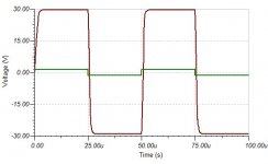
This one is my attempt to improve (hopefully 🙂) the amps slew rate, base design was Valery's at post #51
What do you think guru? Sorry I had to hold on for a little longer before launching into a final build. This is my last DIY amplifier.
I have read Robert Cordell's Mosfet based amplifier and I have adopted the concept of LED as the thermal sensor and surprisingly it shows a lower THD too.
Simulation graph is taken at amps full power.
Cheers!
Albert
I'm back 😀
This one is my attempt to improve (hopefully 🙂) the amps slew rate, base design was Valery's at post #51
What do you think guru? Sorry I had to hold on for a little longer before launching into a final build. This is my last DIY amplifier.
I have read Robert Cordell's Mosfet based amplifier and I have adopted the concept of LED as the thermal sensor and surprisingly it shows a lower THD too.
Simulation graph is taken at amps full power.
Cheers!
Albert
Attachments

Another one 😀
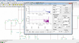
I was inspired to work again with the schematic at post #2, i wanted to know which design, will give me the edge and have it validated if it actually follows the design principle/topology. Not an expert here so the design may contain errors. To my knowledge this one is actually made (in schematic) by member CBS40 and Bimo (Bimo's design was a complex one). Attached also was an opamp looking design that I found and actually pushed me to simulate my circuit revision.
Feel free to point out mistakes and further improvement.
Simulation graph is taken at amps full power (near clipping level).
Cheers!
Albert
Attachments
post56:
Add some local decoupling after the supply rail diodes.
post57
-2.93mA does not match 2*1.36mA !
Could the base currents of T1, 2, 5 & 6 account for the difference of 0.21mA?
and add some local decoupling near the front end.
Add some local decoupling after the supply rail diodes.
post57
-2.93mA does not match 2*1.36mA !
Could the base currents of T1, 2, 5 & 6 account for the difference of 0.21mA?
and add some local decoupling near the front end.
Hi, Andrew,
yes you are quite right, in the cascaded schematic (post #57) there exists a few ma imbalance at the input differential, ...will correct that one. I just hope I am not overloading the VAS, that is some 15ma...
yes you are quite right, in the cascaded schematic (post #57) there exists a few ma imbalance at the input differential, ...will correct that one. I just hope I am not overloading the VAS, that is some 15ma...
Hi, Andrew,
yes you are quite right, in the cascaded schematic (post #57) there exists a few ma imbalance at the input differential, ...will correct that one. I just hope I am not overloading the VAS, that is some 15ma...
It seems the circuit in post 56 has better (simulated) distortion figures than the more involved one in post 57 and that the threshold of clipping for the latter arises at a slightly lower output power.
Perhaps you might ask yourself how well do your developments compare with Valery's "Blameless" into 8 ohms at the same output levels - say at 30 watts and respective clipping thresholds.
- Home
- Amplifiers
- Solid State
- IRFP240/9240 Amplifier (simulated on TINA)