The going rate from Mr.Subramaniam seems to be less than 50 paise per sqft, finished board with solder mask and legend printing. In fact, you shouldn't be all that surprised at this price, considering Rahul's friend from Lucknow or Kanpur has given him rates which are lower. (Rahul had quoted those rates in per-sq-inch, but I converted and checked.) 🙂Originally posted by corbato At Rs. 25 /each you can’t be serious. Comom,,…I buy copper laminated board for Rs. 80/sqft. More power to you and your PCB guy. 🙂
In fact, the exact rate Mr.Subramaniam quoted was less, but the precise figure depended on whether it was 2-ounce or 1-ounce Cu, and on the volume (I asked him for 25 pieces and 50 pieces). I have a feeling also that the JLH PCB will be twice the size I'd discussed with him (I'd discussed a Gainclone PCB, 9cm x 4cm, with him.) Still, all these considered, the rate is less than 50 paise per sqcm. Assuming that each mono PCB will be a (liberal) 6"x4", we're talking 150 sqcm here. This means Rs.65 per PCB if we get just four made (he charges a flat Rs.250 lump-sum for prototype PCBs of quantity three or four, for small size single-sided stuff). And if we order larger quantities, we're talking of perhaps Rs.40-50 per PCB. JLH PCB at one USD each.... anyone? 😀
We should go in for 2-ounce copper, what say you?
I'll any day opt for wider tracks and a slightly larger PCB than vice versa. We're not in commercial production, where every rupee of cost cutting matters. 🙂The JLH site has a PCB layout for the revised amp. It looks a bit wasteful to me. However, if we are thinking in terms of redoing the layout, then caution must be exercised in respect of track width. Should be sufficient for high current draw.
FWIW, I too feel this way. Not because of the quality issues as much as for flexibility issues. My requirements from any power amp PCB will be:Your point on whether we should have plug’n’play type pcb is something that has been bothering for a long time. I think I’ll compromise and go for simple solder posts wherever possible. The quality and fitting of connector we get in the market is just not upto audiophile standard. I’d have like gold plated contacts. And RCA directly into the PCS is strictly no no.
- All the OPS power transistors must be along one edge of the PCB, for heatsink mounting. (I've seen some PCB layouts, including Randy's, where he keeps them half on the left, half on the right, so that he can put two heatsinks on two sides. I don't want such layouts.)
- Two mounting holes, one on each corner along the edge where the OPS transistors mount. These holes will let me use L-brackets to fix the PCB to the heatsink.
- Preferably, all power rail connectors and signal connectors on that edge of the PCB which is opposite to the heatsink edge. (Many of Randy's PCB layouts have power rail inputs on the side edges of the PCB, not the "front" edge. I'd have preferred them all in front.)
- Provision for 0.2" spacing pads for the high-power connectors, so that people who want to use screw-type terminal blocks may do so, and others can directly solder the hookup wires onto the PCB. For signal pads, spacing should be 0.1", and preferably each signal link should have two such pads. (This allows us to run two wires in parallel to the terminal block, in case one of the terminals develops loose connections or corrodes. These provisions are easy to ignore for those who don't want them... just solder directly instead of using terminal blocks.)
- Wide tracks, largish solder pads, and multiple links to star ground wherever needed, so that one can eliminate any ground loop type problems. (One of Randy's OptiMOS PCBs has four separate solder pads to connect separately to an off-board star ground point, for instance.)
Me novice, so I usually find that anything other than bridge+caps is better done using a PCB. So I too would like a PCB for PSU, if possible, please. And I'm open to one PCB for both rails, or separate PCB for each rail... you choose. For the power amp, I certainly want a mono PCB. If I need two channels, I'll take two PCBs. That way, ground connections too remain very clean.I will also prefer to have PCB for the PS, because it will be a current boosted or capacitance multiplier design.
My need for mono PCB for power amp is very simple: I'll only use the JLH for a bi-amped or tri-amped speaker's tweeters. I feel it is too low-power for any other application (I'm not into super-efficient horn speakers.) Hence, in one chassis, I'll always have only one JLH amp, hence my difficulty with a stereo PCB.
Valid points Tarun. I fully agree with you. PCB here appears cheaper slightly but again considering solder mask , roller tinning. legend printing it will come to same so it is best they are made at Mumbai. I know finish there is much better than what I get here.
Wider tracks and pads are simple eough requirements to accomodate on board.
Another small point I would mention is leaving trace in solder mask of PSU rail and amp supply rails so that they are further reenforced while under going roller tinning.
I also suggest mounting output devices on the edge using L bracket as it gives us flexibility to use different type of heatsink.
I feel one common board can be made for both the power rails let me try working out a board this will give some refrence points to start with.
Regards
Rahul
Hi,
Can we put some sort of protection in the amp. Especially turn-on thump. I need to hook this up to the tweeter. If one of you can look thru the circuit provided by ESP, can you comment on how good it is & if it could be added to the project ? You know what, we should probably give it a name.
OK, from what I understand one person gets the PCB made & we do a group buy for the transistors or is it still undecided. Rahul, are we all getting the heatsinks & caps from your source. I would like to build 2 of these. I'm sorry but can't contribute much in terms of technical debate. Any other help I can provide please let me know ?
Ashok,
You have a tube X/O ? What does it sound like ? How difficult to build ? 2-way or 3-way ? What parts reqd. ? Regarding the active X/O we can take it off this thread if required.
Cheers,
sunil
Hi,
Link to the protection circuit by Rod Elliot. Please comment.
http://sound.westhost.com/project33.htm
Cheers,
sunil
Link to the protection circuit by Rod Elliot. Please comment.
http://sound.westhost.com/project33.htm
Cheers,
sunil
Sorry about my ignorance, but I didn't understand what you were referring to here. Can you please explain? Did you mean that while making the PCB, the tinning of the entire tracks should be done first, and then the solder mask applied? That way, the tracks will carry a complete tinning layer along their entire lengths, and this will increase their current capacity?Rahul said:Another small point I would mention is leaving trace in solder mask of PSU rail and amp supply rails so that they are further reenforced while under going roller tinning.
And it's better that we become fanatical about current carrying issues now, because for a Class A amp, I think the sheer steady-state current loads will stress out a PCB which would have been fine for a Class B.
protection circuit
I remember looking at Rod Elliott's circuit and having some minor cribs against it, but I don't remember now what those cribs were. They were minor anyway, and in any case his discussion about the power rating and value of the inrush-current-limiting resistors is lovely.
At the risk of sounding like a stuck record, 😀 can we also look at a Randy Slone circuit for this? His circuit (in his book) doessunil said:Link to the protection circuit by Rod Elliot. Please comment.
- in-rush current limiting
- speaker muting for a few seconds using a relay in the amp output path, to eliminate any turn-on thump
- heatsink temperature sensing (using an NC thermal switch, which is not easily available in India) and protection
- protecting the speaker against any DC at amp output
- visual indication of status using a blinking/steady LED
I remember looking at Rod Elliott's circuit and having some minor cribs against it, but I don't remember now what those cribs were. They were minor anyway, and in any case his discussion about the power rating and value of the inrush-current-limiting resistors is lovely.
What OPS device?
What OPS devices? Will we freeze on the MJ15003/4?sunil said:OK, from what I understand one person gets the PCB made & we do a group buy for the transistors or is it still undecided.
Psoted by tcpip:
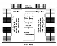
I have attached a proposed layout. This has been playing in my mind for almost a year now. Have a look.
Rahul:
The above addresses some of your views too.
Mr. Subra sounds ideal. Not only his rates are cheap, he appears to know the trade. I've had encounters with PCB makers but none of them knew about 1 or 2 ounce Cu business. Besides, Tarun's experience has been very good with him.The going rate from Mr.Subramaniam seems to be less than 50 paise per sqft
Obviously. So another, group purchase plan? ehh. Hope no unholy men screw this up 🙂We should go in for 2-ounce copper, what say you?
Boss we are gonna use TO3 devices. More traditional approach of mounting the MJ's on the heatsink, rather then a "L" Bracket should be adopted. But I agree that the PCB should be mounted on the Heatsink with 4 suitable spacers.All the OPS power transistors must be along one edge of the PCB, for heatsink mounting.
Track to the grounplane should be as short as possible. Even a seemingly short length of track has resistance.Wide tracks, largish solder pads, and multiple links to star ground wherever needed, so that one can eliminate any ground loop type problems.
Yes.With this mounting strategy, I'd prefer to have the RCA sockets and other things off-board.
Each Channel will have its own power regulating board. For both the rails. So total 4 boards for the '+' and '-' rails. Even the transformer will have two secondary of 25volts each,So I too would like a PCB for PSU.
I have attached a proposed layout. This has been playing in my mind for almost a year now. Have a look.
Rahul:
The above addresses some of your views too.
Attachments
Sunil/Tarun,
I'd not really want any protection device/circuit in my audio patch. A non-linear additional like a fuse or relay contact will be strictly no no by me. i'd rather run my amp sensibly and take all due care.
Sunil,
Actually the Tube Xo is easier to implement and listen to 🙂 Just 2 tubes and a few resistors/caps. I have the schematic somewhere. Will email to you if desired.
Tarun:
Yes MJ15003. And quite a techno guy you are 🙂 Blinking LED's and such 🙂
Sorrycorbato said:Boss we are gonna use TO3 devices. More traditional approach of mounting the MJ's on the heatsink, rather then a "L" Bracket should be adopted. But I agree that the PCB should be mounted on the Heatsink with 4 suitable spacers.
 I should have remembered that my L-bracket thing is less of a necessity if one uses TO3. But can we please at least do it such that the PCB design assumes TO247 devices, and puts all OPS devices on one edge of the PCB, and we then are free to use either TO247 or TO3 devices (with short wire leads from TO3 to PCB)? That way, one can even use the PCB with the Toshiba TO247 BJTs someday if one wants to.
Looks cool. I'm in!I have attached a proposed layout. This has been playing in my mind for almost a year now. Have a look.
The chassis layout will not have much of a bearing on my plans, unfortunately, because I want to build active speakers, hence my chassis will combine multiple amps of various types. But this is incidental. The point is that I'm in. Slurrrrp! 😀
Hi! Friends,
We cannot expect all fingures to be equal in all respect. Here then there would be a deadlock. It is the genuine interest and participation that matters. Your constructive attitude alone is highly appreciable.
The protection from ESP is simple and good but again relays in signal path are not preferred in high end audiophile setup. One can always use this relay to switch off the amp mains but this being class A one the capacitors alone would have sufficient charge to damage the speakers in event of any failure. If you wish the protection ckt is simple enough to be wired on a Vero board , I can do the same for you no charge but only when you finish the Amp.
Tarun and Ashok
The semiconductors will no doubt have to be a group buy. Capacitors I can get but remeber they are untested as yet for serious audio application however 2 each per amp can be bought as extra as they will cost max Rs100/ they also can be given a try.
TO247 pads on PCB provide easy adaption to any type of transistor mounting ie wether direct on heatsink, thru L bracket or TO3 on heatsink.
Ashok now what ever they say abt India shining I see experience shining. Fantastic layout. One more point of interest that these heavy version of heatsinks are available in plenty at Agra and small sections can be combined to cater for all devices ie in output or the power supply. We can easily get an ms section frame made. All heatsink cut to one size and mounted all around. Finish it off by a cover and a good Al dial. Simple and practical.
Perhaps its time we looked at active devices also.
Regards
Rahul
Originally posted by Rahul
The semiconductors will no doubt have to be a group buy..Capacitors I can get but remeber they are untested
I propose that all semiconductors should be ordered from On Semi. They may not have some small signal devices. These could be procured from RS. Resistors from RS too.
That was just a quick rendition. Our final design will need to be much more polished. It will be.small sections can be combined to cater for all devices ie in output or the power supply. We can easily get an ms section frame made. All heatsink cut to one size and mounted all around. Finish it off by a cover and a good Al dial. Simple and practical.
The Heatsinks housing the OP devices will be thermally connected to each other. "L" type AL angle will be bolted to the top and bottom. Left and Right Heat Sinks will be bolted to the AL front panel and again a "L" channel fabrication in the back.
I just had an idea. In an earlier thread Tarun had proposed that we should first prototype and then firm up on a layout which then everybody will adapt. I volunteer to do the prototyping. I have almost all type of metal working tools at my disposal and it will be easy. You will need to tell me what kinds of Heat Sink profiles are available. Also, their rating. It of-course quite easy to to determine that once you have their physical dimensions such as length, width, # of fins, their height etc.
such as?Perhaps its time we looked at active devices also.
Cheers
and BTW did you see the pic of those excellent Knobs Tarun sent me and others? They are posted in the other [INDIA] thread.
PCB making process.
Tarun:
This one not only for you but others who may be interested in PCB manufacture procedure
A glance alone says lot abt the PCBs you got made there good stuff. Well let me tell you in brief about the PCB making process.
There are two different methods:
1 Screen printing and etching (simplest)
2 Photo transfer
Screen printing:
This follows the same process involved in common printing of visiting cards a positive of artwork is made and a screen frame is exposed. Using alkaline soluble ink incidently called PCB blue the pattern is transferred to copper clad board. This is now etched in ferric chloride solution. after all unwanted copper has been etched the board is washed and holes drilled. Another screen is exposed that has only pad outline if possible of slightly bigger size than pads. The solder masking heat resistant green paint is once again printed this covers whole of the PCB except the areas that need to be soldered. The PCB is now passed thru roller tinning machine that has a par of rollers running in molten solder, the solder sticks to the cleared areas ie ones that have to be soldered. A thick layer of solder results in soderdripping and collecting on edge.
Drawbacks are only coarse design can be made. Secondly the copper layer is weakened as it undergoes etching process. Manual time consuming, wastage of copper.
Photo process:
The laminate is either ready photosensitised or coated with suitable chemicals. Generally this material available in spray cans. The photosensitive board is now exposed using the artwork on transparent films. This is then etched and similar procedure follows as in above mentioned process. Advantages track is very sharp high precision. Expensive., requires individaul care for each board. much copper is wasted in etching process.
PTH: ( Plated Thru Holes)
This way true industrial and high end PCBs made .
A double sided copper clad laminate is first drilled using the NC ( Numeric Control) file generated by the CAD software. These machines have multiple heads and all holes are drilled in one single operation for extra
The drilled sheet is put into a copper solution and copper is deposited between the sheets thus creating thru plated holes.
A thin film is deposited using proprietry sheets from firms like 3M. This covers the holes as well as tracks. Now using electrolysis undesired copper is removed. The coarse PCB is now put in another solution and a layer of lead and tin is deposited re -enforcing the tracks. Solder mask is now printed as in screen printing.
Advantages high precision, use less copper to start with, all material dissolved can be recycled, uniform layer of tinnig,automatic process.
Boards made this way are rugged, just try removing a chip from PTH board. Tracks are hard, try one cutting on a PTH board.
Tarun most of the time, board with less copper ie fine layer is meant for PTH fabrication, ie more tin and lead has to be deposited later but being industrial grade this is the more that is abundant as industrial scrap. Small time PCB manufacturer buy this to compete in mkt, etching process further degrades the copper layer. As you rightly recognised knowledge of PCB manufacturer is also of prime importance for geting a quality PCB made so is the awraeness of the manufacturer.
Now for your query on the track solder deposition :
A common example is the SMPS PSU of PCs now this has 20Amp at 5V current conductor. The tracks are solder plated. This does not means that we apply solder to thicken it.
Before roller tinning areas are left on tracks that exposes copper despite there being no connection here this causes solder to be deposited during roller tinning enhancing track thickness and current carrying capacity. Same technique I suggest applying here too for high current supply rails.
Another point worth mentioning the PCB can be made as simple layout with short path to the ground. I would like to mention that in RF application this is all the more critical and we use the technique called maxima ground plane ie all unetched area is filled with copper this results in enhanced stability and screening. I am sure I have sure I have seen similar technique adopted in some very high end stuff. No problems at all for me to do the same here.
Getting long and some may say off topic but again part of the project. If it is helpful in any manner then I am higly obliged if waste of BW then kindly skip.
Regards
Rahul
Hey DIY Gods,
I'm in for 2. The chassis layout looks cool, really mean actually, with the heatsinks on all 3 sides. If it is a dual mono will there be space to put 2 transformers next to or behind each other.
MJ15002 - If we are going in for these, aren't there other's at the same price point. I'm not sure onsemi will deal with 20 pieces. The table shows an approx of what is available. They have been chosen from what I have read of recommendations. They all seem to be compatible. I could be wrong, so correct me.
Part No. Price
Digikey Futurelec Electronix
2SC3281-O-ND 2.48 1.89
MJ15003OS-ND 3.51 1.75 5.33
MJ21193OS-ND 3.75
MJL3281AOS-ND 4.46
MJ 15022/15023 3.9
2SC5200/2SA1943 4.25
Rahul/Ashok - Protection circuit. Is there a simpler setup I can use, if not the ESP layout.
I'm not aware of the specs of the design you guys are discussing. Can you point me somewhere I can ogle at the figures ?
Ashok, yes, please send me the schemo. I'd like to see it & try if possible.
Tarun, George called & said the knobs had arrived. I'll be picking them tommorow.
Cheers,
sunil
Shoot, the table messed up.
It was the price from 3 vendors, of different transistors. Anyway please see if it helps. Price for a single unit for the MJ15003 varies from 1.75/- from futurlec.com to 5.33/- at electronix.com. The MJ15022, supposedly an upgrade of 15003 is going for 3.9/- from futurlec.com. At 45 bucks to the dollar, that is Rs 350/- for a complimentary pair.
Cheers,
sunil
Hey Sunil!
Got caught with the other long post on PCB just saw missed your name at start of the earlier post abt protection and stuff. This design is good and simple enough anything extra would be a dethump ckt incorporated within.
Again I am sure you all would excuse the slipups as well as spelling mistakes, considering the fact that I do the surfing at night when my wife and Kids are taking a nap. Now dont U all know Dakoo bhi biwi se darta hai.
Good stuff abt the BJT devices Sunil. Ashok that was what exactly I meant we need to fix the small BJT choice weather the BC series devices or the 2SC jap stuff. Again given Sunils option the final output devices also. Tomorrow I also check the devices avbailable here in local mkt. The layout for the PCB has begun.
Let me be of some help to friends I get few boards made along with my commercial PCBs for trial , once done we finally freeze the layout. Now a headcount for the Beta run.
Regards
Rahul
Samples from OnSemi?
I believe one can order up to 25 of each type of device from OnSemi, and they charge only the courier charges, and deliver anywhere in the world. That way, we can get the MJ15003/4 or successors. Customs Duty is of course to our account.
I believe one can order up to 25 of each type of device from OnSemi, and they charge only the courier charges, and deliver anywhere in the world. That way, we can get the MJ15003/4 or successors. Customs Duty is of course to our account.
Hi friends,
Took a tour of local mkt. The 2Sxxx series devices do not appear very common what do you say suggest should I complete the PCB with BC and BD devices.
LOoking forward to your suggestion.
Regards
Rahul
Took a tour of local mkt. The 2Sxxx series devices do not appear very common what do you say suggest should I complete the PCB with BC and BD devices.
LOoking forward to your suggestion.
Regards
Rahul
Tarun:
Custom is not a problem with samples. I regularly rcv from TI, On Semi, National, AMD.
Rahul:
Both the 2SA devices are available from RS India. Should be cheap.
Edit: aaach... 2SA1358 is not listed with RS. Sorry
Custom is not a problem with samples. I regularly rcv from TI, On Semi, National, AMD.
Rahul:
Both the 2SA devices are available from RS India. Should be cheap.
Edit: aaach... 2SA1358 is not listed with RS. Sorry
Ashok,
If they are available from RS India why don't we go ahead & buy them. I wrote to the RS India people for MJ15022 for an amp I have, that needs repairs. It looked like a quote, they asked for my house address, got a mail saying "We have received your request & will reply shortly". After that nothing happened. What is the experience you guys have had ?
Tarun,
Sorry about that. I did'nt know Onsemi will sell 25 units. The search turns up with links to their distributors. BTW, the knobs are beautiful. Thankyou for tha same. Any idea how I can get an indent or marking made on the front face.
Cheers,
sunil
- Status
- Not open for further replies.
- Home
- Amplifiers
- Solid State
- [INDIA] Group Amp project