Very good work Barry, those cameras need dailigth, but i can see quality
As i have those kind of cameras and i know they do not define.
Pretty boards, and you decide to use Hi Speed Diodes and pretty big electrolitic condensers....good that...the amplifier need big filtering because of consumption is big too...not to produce low frequency noise into the rails..i am using 15000 each rail..i can see that you are using more...Goood.
Now Barry, GEM is very near to be guaranteed 14 times!
Oh!..i was forgetting.... better to use a resistor in series with the extra NPN transistor...the one is always in classe A...with 1 ampere or more flowing...the adjustment there is not so easy.... carefull with your movements...and fix your meter cables, measuring DC voltage over this resistor extremes.
You can use the one you have...0.1, or 0.22.... 0.33 ....0.47 or even 1 ohm...and use ohms law to calculate current.... fast switch on and off...and install limiting current rail resistors.
I am using a 200 Volts and 16 Amperes unit in that position.
regards,
Carlos
I had posted my version of PCB for the GEM in post #322 of this thread. I assembled the board and tried to test it this forenoon. I was seeing +14volts DC on the output. I simply could not up the bias from what minimum current was flowing ie., 23 mA.
I checked thoroughly and guess what I found!! All driver and Vbe transistors of mine are in TO220 package - 2SC4883 and 2SA1930 - the pinout being BCE; but I had assumed that the transistors that Graham used were TO126 and have done ECB pinning on the PCB.
Fortunately there was no smoke or any visible damage. I am going to snap the Base and Emmitter leads and criss-cross them with insulated wire to make the connection to the PCB. Let us see if this works well since I am hoping that nothing is damaged.
SO IF ANYONE IS USING MY TRACK PATTERN FOR HIS OWN PCB, please bear in mind that the Driver and Vbe transistor pinning is ECB.
Hi Samuel,
I'm keeping my fingers crossed for you.
BD139 + 2SC3421 = e-c-b
2SC4793 + 2SC4883 + 2SC5200 = b-c-e
______________________________
Barry has had other commitments recently.
His prototype pcb is populated and mounted against a completed heatsink assembly, but we shall have to wait until he returns refreshed from his holidays before learning of his tests and audition findings.
Cheers ......... Graham.
My first GEM construction simply did not worked!
And i check several times.
The problems when we make our mistakes, is that we can watch an transistor (i can!) wrong, and check it as correct many times...so...start some vicious repetition of checks without result...something alike dog trying to catch it's own tail.
I learn that the better way is to remove all parts...first the active components, and measure each one outside the board.... and them i had found PNP in the place of NPN and other mistakes...this is so common here that i used a good name as my identification...Destroyer Extra...because i use to destroy a lot of parts making mistakes.
Result of that was the development of a rule: "never try to figth against yourself...recognise your week point and do it again since the beginning"..... this rule, made customized to me, is reducing my time waste with hidden (to me) mistakes.
The Second assemble runned perfectly, and the third work the first power on, that one i did not need to adjust nothing, already had experience enougth, and trimpot already in proper position.
It will work.... those strange dark clouds will disappear, and an enormous smile will appear in your face when start to listen, the GEM, in my point of view, a precious stone.
regards,
Carlos
Graham, Carlos,
My mistake due to presumption of transistor package and hence, pinout is not something that I have encountered earlier having made numerous PCBs for many designs out there and some of my own. But I do feel bad if by chance someone has put in efforts in making his/her own PCB using my layout as a guide.
Today I snapped the Base and Emmitter leads of all driver and Vbe transistors and using silver plated cable with teflon insulation I connected the wires criss-crossed into the PCB holes.
Graham, I have used 2SC4883A in the Vbe position as well and not BD139. I guess it is O.K.
With Class-A trimpot set to a minimum and Class-AB trimpot set to 50% I switched on the amp with 22 Ohm resistors in both rails; I measured an offset of 1.2mV at the output and Iq of 43mA. So I don't think that any damage has occured.
I just have one question. Since both my Multimeters can only measure 200mA and the 10Amp range is not working O.K. is there some other way of measuring and setting the bias - first 400mA for Class-A and then adding another 100mA for the Class-AB helper making a total of 500mA.
Setting 400mA for Class-A by measuring the voltage drop across the 0.1E resistors of the output devices is a possibility but then how do I measure the added 100mA for Class-AB? Maybe a low value resistor in the supply line and measure the voltage drop?
Can Graham, Carlos or anyone else suggest the safest and easiest way to do this given the limited range of most Multimeters?
Hai all,
One more issue is that the transistors that I am using, ie., 2SC4883A and 2SA1930 are both with plastic back/insulated type. When 2SC4883A is used in the position of Vbe multiplier as well, as I have done in my present test set up, will the additional thermal resistance of the plastic back result in a lag in thermal tracking and therefore, inadequate thermal compensation?
Can someone please point me to biasing details (I already have Graham's write up) in the scenario where multimeters are not able to measure more than 200mA DC? And the thermal compensation question above.
Thanks,
Samuel, as Graham is busy, i will try to help you
Install a 1 ohm resistor into the Class A extra NPN transistor, the one that always have around 1 ampere crossing it.
Because of ohms law calculations, when you have 1 ampere crossing some resistor, will appear, as consequence, a voltage that can be measured by our standard multimeters....you have to adjust to measure something around 1 volt..... then you remove keep the resistor for a while.
You may have, already installed, series resistor connected to positive and negative rails...series connection related the supply...let's imagine that you used 5 ohms resistor.... you will measure voltage developed over it, and this voltage is the entire current that is flowing into the amplifier....in the reality, each resistor will show you half amplifier current consumption...the upper half...and the lower half...observe that this current corresponds to lower amplifier halve... will be measured over the negative rail resistor.
Will already appear there 5 volts...because 1 ampere is crossing this resistor (ohms law).....
Now you must adjust the other trimpot, the main bias trimpot...the one at the amplifier middle, to introduce MORE, 250 miliamperes of consumption to both rails...this is the class AB biasing, and it will be started with bias zero...and you will increase till have this current.
Well...really confused...as you will perceive.... that you will finally have more iddle consumption to lower amplifier half than to higher amplifier half....it is OK!
More details, some doubts, check with Graham.... call him and wait for him...he is more skilled than me.... he is the designer..i am only his friend.
If you have patience enougth...this thread already has this informations..the problem is that we change our mind....hehe..improvements!
regards,
Carlos
Hi Carlos,
Thanks for keeping things going until I get a chance to answer.
Hi Samuel,
There is nothing wrong with putting a 0.1 ohm resistor in series with say the positive rail supply to the positive fuse.
400mA will drop 40mV; then 500mA - 50mV. Then recheck after running loud or after one hour.
If the output stage Vbe bias setting transistor is not wholly on the heatsink (ie soldered to a pcb), then the tracking is likely to be inadequate because of undesirable thermal conduction out through its leads. Body insulation makes construction more simple and should not be a problem.
Some designers bolt their bias sensing device to the back of a power transistor via thin connecting wires, but my recommendation of everything after the first four transistors mounted on to and hard wired on a convection cooled heatsink does work.
Cheers ......... Graham.
Thanks Carlos and Graham for your most needed answers. I am going to use BD139, BD140, MJE3055 and MJE2955 to do the initial setup. Last night while trying to set the bias I lost both the lower half 2SA1943 transistors. It could be due to the earlier wrong connections of all 2SC4883A and 2SA1930 transistor Base and Emmitter connections getting flipped due to TO220 package of these transistors and my PCB being configured for TO126 lead out and in the process probably causing some secondary breakdown in the semiconductors.
However, the excitement to hear the GEM is not smothered. I will try the cheaper transistors initially and then switch over again to the more expensive faster transistors. Will keep you all posted.
Thanks again,
However, the excitement to hear the GEM is not smothered. I will try the cheaper transistors initially and then switch over again to the more expensive faster transistors. Will keep you all posted.
Thanks again,
Samuel, in my mind, the most important part in this amplifier, is the rail protective
resistor....because this amplifier has not current limit, so, you can adjust till the transistor explode....you can increase bias till the transistor destruction.
So, some limiting resistor will be needed, in your case, using 3055/2955, it may be, at least, 5 ohms, to limit the maximum current entering the circuit board at 6 ampéres when board has short circuit between rails, shorted components or bias trimpot turned all the way up to the wrong side.
During adjustment, i suggest you to use another 5 ohms (or a little bigger) into the Class A transistor, the one is down the amplifier, near the negative rail.... this one can be more easy destructed by excess of biasing.
Graham did not constructed this amplifier to produce a Kit....if was a kit, many protective devices had to be included, to avoid this possibility of mistakes, as Kit builders do not have the obligation to have Post Graduation (PHD), to be Doctored related electronics.
You see, dear Samuel, that even the supply invertion diodes are omitted, they are not there, as this is not a kit.
We, diy as you are, normally we have some practical experience to avoid those problems, but even this way, i use to burn a lot of things here too!
Please, include your rails protection resistor during first power on when modifications where made, or repair made.... the current will be the voltage you will measure over the resistor extremes divided by the resistance value you put as rail protection.
Remember that Voltage may be expressed in Volts and current expressed in ampéres.....so....900 miliamps will be expressed as 0.9.....well...you may know that better than I...but is not offensive to remember and try to avoid you to forget those basic practical things.
All your efforces will be paid to you, with pleasant audition, as this is a very good amplifier...Guaranteed!.... and i will never tired to say that Aksa, Symassym and GEM, are my prefered amplifiers.
regards,
Carlos
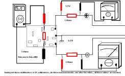
Here is a Sketch, if you already know, i am sorry .
But there are others that do not know how to do it.
To avoid that Doctor Boerer Detailer enter to say that Multimeter polarity is wrong.... i already observed that.... so...users!...if pointer did not move forward...invert polarity please.
regards,
Carlos
But there are others that do not know how to do it.
To avoid that Doctor Boerer Detailer enter to say that Multimeter polarity is wrong.... i already observed that.... so...users!...if pointer did not move forward...invert polarity please.
regards,
Carlos
Attachments
Carlos, so you mean that I have to break off the lower NPN emmitter connection to negative rail and insert the 5E resistors and then measure the voltage drop across it?!
Yes, i think so Samuel...the 5 ohms choice was a 7 amperes limiting choice
To avoid unbalance output voltage, do not include speaker for a while.
You can use 0.22 ohms, 0.33 ohms, 0.47 ohms, 1 ohm, 2,2 ohms, 3,3 ohms, 4,7 ohms....in other words, you can use the one you have in your "precious material box".... the lower it can be, better to keep amplifier balanced related output voltages...because, using 5 ohms...if hardly driven, as a mistake related bias adjustment, small voltage will reach amplifier using this junction emitter to collector...using others, not so big value, despite dangerous, are more precise method, that will let you in peace, not needing to retouch adjustment again when removing those auxiliary, series protective resistors.
Again, the voltage developed over the resistor have to be divided by this resistor value, expressed in ohms...to obtain the current without the danger of open the circuit that can cause accidents, as wiring have some spring capacity to produce shorts!... some position "memory".... the desire to return to it's normal position, the one the wire was before you move it.
Using those resistors i told you, the voltage you may adjust, measured over the included resistor that is in series with NPN, Class A, output circuit.(Colector to emitter circuit)
0.1 ohms................ voltage to be measured is 0.1 volts, or 100 milivolts
0.22 ohms.............. voltage to be measured is 0.22 volts, or 220 milivolts
0.33 ohms.............. voltage to be measured is 0.33 volts, or 330 milivolts
0.47 ohms.............. voltage to be measured is 0.47 Volts, or 470 milivolts
1 ohms.................... voltage to be measured will be 1 Volt
2,2 ohms................ voltage to be measured will be 2,2 Volts
3,3 ohms................ voltage to be measured will be 3.3 Volts
This is the "exclusive" class A transistor 1 ampere biasing... above values, are made for beginners, not exactly for you, but for many guys that will print that to turn easier their work without calculators or brain made basic Mathematics.
As positive supply rail will have 0.250 A, or 250 miliamperes...that is 1/4 of the class A biasing current....all values of voltage you will have above, will need to be divided by four.... when voltage measured was 1 volt..... your real result, beeing positive rail, will be 250 milivolts (O.250V).
Yes!..i know you are not an idiot...the purpose is not to explain basic electronics to you, as you may be experienced, this is directed to young diy students, beginners...so explanation is so...so...so....so...let's see..hummmm, detailed.
regards,
Carlos
Hi Samuel,
The only way you could lose the 2SA1943 is if they are driven 'on' too hard.
Could be a shorted pnp driver transistor, or a shorted npn VAS transistor.
Or if the amplifier is immediately oscillating due to layout not being as recommended.
I would reduce rails to +/-25V for the older BD/MJE you wish to try.
I recommend trying first with 22 ohm resistors in place of fuses to check output zero without any bias or load.
Then fit 0.22 ohms in series with quick blow 6A fuses and very slowly set up the bias without any load.
If okay, back off the bias, remove the 0.22 ohm resistors and set up the bias again.
If okay connect up an output load resistor and see if amplifier runs with an old speaker.
As Carlos says - there are no current limiting devices - I don't like the way they can interfere with full range reproduction.
Also Carlos was correct earlier - it is essential that you check every device after a mistake has been made - akin to starting afresh.
Cheers ......... Graham.
When you appear, dear Graham, you remove heavy weigth over my shoulders.
As it is not easy represent you, having my practical know how, we need you tracking this thread.
Good that i could represent you for a while, without make mistakes.
But now i feel relaxed..."the man", arrives.
In my point of view, nothing less than:
Our Majesty, the diy King of United Kingdon, and surrounds!
regards,
Carlos
Carlos and Graham, first of all I must express how much I appreciate your attentiveness and patience. Thanks a ton.
Setting up the GEM is quite different from all other amplifiers I have made thus far. Normally only adjustment of the Vbe pot and output null is required in most amps.
Graham, any of the causes you have cited cannot be ruled out. Oscillation - it is a possible case. With 22 ohm resistors in series with each supply line followed by insertion of 1.5Amp fuses in parallel with these resistors (yes I was lazy to desolder the resistors) still gave me 1.2mV DC at the ouput. I placed a multimeter in series with the positive supply (switched to 200mA DC range) and this was showing overflow at every instance of being powered up but everytime settled down to 43mA DC.
This is where I made the blunder. Without monitoring the current of the lower NPN transistor I tried to adjust the 100E Class A trimpot. The ammeter in the positive line would show an increase of current till about 100+ mA and go to overflow (ie., above 200mA DC). I backed off everytime and each time this was repeated the results were identical. There were no signs of heating up nor was the output offset varying from 1.2mV.
I backed off the bias, the ammeter in the positive rail was showing 43mA. I tried to measure the voltage drop across one of the upper 0.1E resistors. The moment the voltmeter probes made contact with the resistor leads, the negative rail 1.5Amp fast blow fuse broke and both the 22E resistors went up in flames. I immediately pulled out power to the test jig.
Hence, I think it must be oscillation that caused the current to abruptly jump from a little over 100mA to over overflow in the 200mA range each time and the voltmeter probe must have caused a burst of oscillation even at minimum current draw.
I will post a picture of the assembled board. The layout and assembly are too good to cause any oscillation. Even the 0.1E resistors are made of 10 x 1E (2Watt) carbon film resistors. The only two causes could be (i) none of the big caps were bypassed by smaller electros nor film caps even though I have made provision for this on the PCB and (ii) power and small signal grounds have been separated by a 10E 2Watt carbon resistor; so, in the first case high inductance of the big electros could be causing the oscillation or if it is the second case, differential ground potential may be causing the oscillation since this is a high bandwidth amplifier!!
Graham, your recommended method for setting up bias is slightly different from what Carlos is saying. He insists that there should be a resistor of say 5E between negative rail and Emmitter of lower NPN transistor OR between Collector and output node of the same transistor and to measure the voltage drop across this resistor.
Whereas you are recommending 6Amps fuses in series with 0.22E resistors in both the rails and to measure voltage drop across these. I personally (and for no particular reason) prefer your method, but you have advised that the bias should be backed off, the resistors removed and bias set up again. This is were my problem is; once these resistors are removed, I cannot any longer use the voltmeter but have to use the ammeter and the range I am restricted to is 200mA DC.
If I resort to Carlos method, isn't 5E a slightly high value and the wattage has to be quite high. I have lots of 0.1E, 0.15E, 0.22E, 0.33E (all 5 or 10Watts) but they are either fusable type or wirewound and both types exhibit inductance and are known to cause oscillation.
Have I understood both of you correctly or am I missing something?
Hi Samuel,
You are describing an amplifier bursting into RF oscillation as the bias is increased.
This alone can destroy output devices due to the oscillation causing cross-conduction.
I have just studied your pcb layout as per Post#322.
It looks as if you have taken the thick output track alongside the input devices.
This would be likely to cause oscillation in *any* solid state amplifier that is capable of sounding good; ie. capacitive coupling between output and input.
** I did write warning that there should be a gap of say 2"/5cm between the input devices and any parts/wires connected to the output. **
(With correct layout, devices and screening, the GEM circuit is also capable of being used as a high definition video signal distribution amplifier.)
I'd rather use stripboard to achieve a properly functioning amplifier, than having something that looks smart but which compromises performance !
It is also my view that a layout should be tested before time and trouble is taken to fabricate it as a pcb. I was even worried about all the wire lengths on Carlos' 'quick-board', but he did keep small signal input and voltage field generating output connections apart, and thus reduced the chances of capacitively induced RF oscillation.
Sadly, your construction was incorrect from outset, as was Barry's initial pcb suggestions. That is why I drew out a suggested veroboard layout and went on to get Barry to repeatedly change his. I did not realise you were continuing with that layout.
Cheers ......... Graham.
Hi Samuel,
More thoughts.
Are you still trying to implement separate signal input and output stage power grounds ? I mentioned this in Post#302.
How do you know that the (NFB loop controlled) output stage currents are not causing the development of a circuit coupled output stage RF voltage with respect to differential input/NFB sense signals ?
I always believed it essential that all grounds have a common plane or star earth with respect to a input/NFB sensing differential input stage. Maybe your efforts have done no more than prove this.
An amplifier should function wrt signal input and its ground termination alone.
The input ground is *the* operational reference connection and thus power rails should also be directly referenced to this.
Try connecting *all* your grounds directly to the input ground to make a star earth. Also try a 47pF Miller C.dom in an attempt to overcome input/output wiring proximities.
Cheers ......... Graham.
Samuel, always that you find "ideas conflicts" between me and Graham
Do not have any doubts to follow what Graham says.
He is much more experienced than me, related theoric studies and practice work.
Also he is more clever than i am
In some scale from 1 to 10.... Graham may be 9,8 and i am fighting to jump to 5.0.
I have any problems with that!.... this is real, this is full of realism, the truth of the true.
Follow my dear friend Graham, my instructor, my teacher and do not worry about things i said.
"to Ceasar, everything that belongs to Ceasar!"
regards,
Carlos
- Status
- Not open for further replies.
- Home
- Amplifiers
- Solid State
- Incredible quality amplifier by Graham, prepare your ears for it