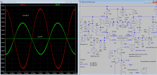
Feedback on one side only, not both side, so either left or right. Feedback from right side is same but slightly worse (need to expand here). The output level remained the same when no-load, 50k load on one side and on both side when feedback on either side. The output from both jfet is about ~20Vp and drop to about ~10Vp when feedback is applied, which translated into gain drop of half in the output level. There are room for improvement, we hope.
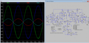
Here is the result of stepped load:
.step param RL list 1Meg 470k 220k 100k 50k 20k
Here is the result of stepped load:
.step param RL list 1Meg 470k 220k 100k 50k 20k
Attachments
Last edited:
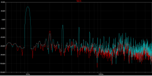
Here is FFT of 50k and 20k (red) load.
Attachments
Last edited:
I've done some simulations and I've found a good circuit.
There's local feedback from driver's cathode to jfet's gate plus gnfb.
I've reduced the current flowing through jfet and 12AX7 to 600 uA and got the following results on 8 Ohms:
There's local feedback from driver's cathode to jfet's gate plus gnfb.
I've reduced the current flowing through jfet and 12AX7 to 600 uA and got the following results on 8 Ohms:
Code:
.step v=0.1
Heightened Def Con from 2.50036e-009 to 4.50036e-009
N-Period=1
Fourier components of V(output)
DC component:-0.0109116

Harmonic	Frequency	 Fourier 	Normalized	 Phase  	Normalized
 Number 	  [Hz]   	Component	 Component	[degree]	Phase [deg]
    1   	1.000e+03	1.983e+00	1.000e+00	   -1.00°	    0.00°
    2   	2.000e+03	9.982e-05	5.034e-05	  154.52°	  155.53°
    3   	3.000e+03	6.797e-05	3.428e-05	  177.64°	  178.64°
    4   	4.000e+03	4.569e-05	2.304e-05	 -178.90°	 -177.89°
    5   	5.000e+03	3.744e-05	1.888e-05	 -179.92°	 -178.92°
    6   	6.000e+03	3.047e-05	1.536e-05	  179.37°	  180.37°
    7   	7.000e+03	2.589e-05	1.306e-05	 -179.99°	 -178.99°
    8   	8.000e+03	2.284e-05	1.152e-05	 -179.88°	 -178.88°
    9   	9.000e+03	2.023e-05	1.020e-05	 -180.00°	 -178.99°
Total Harmonic Distortion: 0.007239%(0.007787%)


.step v=0.2
N-Period=1
Fourier components of V(output)
DC component:-0.0218975

Harmonic	Frequency	 Fourier 	Normalized	 Phase  	Normalized
 Number 	  [Hz]   	Component	 Component	[degree]	Phase [deg]
    1   	1.000e+03	3.966e+00	1.000e+00	   -1.00°	    0.00°
    2   	2.000e+03	2.826e-04	7.125e-05	  129.46°	  130.47°
    3   	3.000e+03	1.624e-04	4.096e-05	  171.85°	  172.85°
    4   	4.000e+03	9.218e-05	2.324e-05	 -173.48°	 -172.48°
    5   	5.000e+03	7.195e-05	1.814e-05	  179.97°	  180.97°
    6   	6.000e+03	6.114e-05	1.542e-05	 -177.77°	 -176.76°
    7   	7.000e+03	5.414e-05	1.365e-05	 -179.90°	 -178.90°
    8   	8.000e+03	4.584e-05	1.156e-05	 -179.72°	 -178.72°
    9   	9.000e+03	4.191e-05	1.057e-05	 -179.88°	 -178.88°
Total Harmonic Distortion: 0.009107%(0.009551%)

.step v=0.3
N-Period=1
Fourier components of V(output)
DC component:-0.0329733

Harmonic	Frequency	 Fourier 	Normalized	 Phase  	Normalized
 Number 	  [Hz]   	Component	 Component	[degree]	Phase [deg]
    1   	1.000e+03	5.949e+00	1.000e+00	   -1.00°	    0.00°
    2   	2.000e+03	6.094e-04	1.024e-04	  116.33°	  117.34°
    3   	3.000e+03	3.665e-04	6.160e-05	  167.93°	  168.93°
    4   	4.000e+03	1.391e-04	2.339e-05	 -172.24°	 -171.23°
    5   	5.000e+03	9.645e-05	1.621e-05	  179.59°	  180.59°
    6   	6.000e+03	9.221e-05	1.550e-05	 -175.91°	 -174.91°
    7   	7.000e+03	7.745e-05	1.302e-05	  179.98°	  180.98°
    8   	8.000e+03	6.904e-05	1.161e-05	 -177.89°	 -176.88°
    9   	9.000e+03	6.248e-05	1.050e-05	 -179.91°	 -178.91°
Total Harmonic Distortion: 0.012552%(0.012883%)

.step v=0.4
N-Period=1
Fourier components of V(output)
DC component:-0.0441409

Harmonic	Frequency	 Fourier 	Normalized	 Phase  	Normalized
 Number 	  [Hz]   	Component	 Component	[degree]	Phase [deg]
    1   	1.000e+03	7.933e+00	1.000e+00	   -1.00°	    0.00°
    2   	2.000e+03	1.088e-03	1.372e-04	  109.54°	  110.54°
    3   	3.000e+03	7.489e-04	9.441e-05	  166.18°	  167.18°
    4   	4.000e+03	1.863e-04	2.348e-05	 -172.19°	 -171.19°
    5   	5.000e+03	1.198e-04	1.510e-05	  178.98°	  179.99°
    6   	6.000e+03	1.235e-04	1.557e-05	 -175.27°	 -174.26°
    7   	7.000e+03	9.709e-05	1.224e-05	  179.80°	  180.80°
    8   	8.000e+03	9.250e-05	1.166e-05	 -177.03°	 -176.03°
    9   	9.000e+03	8.087e-05	1.019e-05	  179.96°	  180.96°
Total Harmonic Distortion: 0.017073%(0.017320%)

.step v=0.5
N-Period=1
Fourier components of V(output)
DC component:-0.0554005

Harmonic	Frequency	 Fourier 	Normalized	 Phase  	Normalized
 Number 	  [Hz]   	Component	 Component	[degree]	Phase [deg]
    1   	1.000e+03	9.917e+00	1.000e+00	   -1.00°	    0.00°
    2   	2.000e+03	1.719e-03	1.734e-04	  105.59°	  106.59°
    3   	3.000e+03	1.348e-03	1.359e-04	  165.20°	  166.21°
    4   	4.000e+03	2.336e-04	2.356e-05	 -172.69°	 -171.69°
    5   	5.000e+03	1.548e-04	1.561e-05	  178.18°	  179.19°
    6   	6.000e+03	1.551e-04	1.564e-05	 -175.07°	 -174.07°
    7   	7.000e+03	1.129e-04	1.138e-05	  179.59°	  180.60°
    8   	8.000e+03	1.161e-04	1.171e-05	 -176.68°	 -175.67°
    9   	9.000e+03	9.797e-05	9.879e-06	  179.85°	  180.85°
Total Harmonic Distortion: 0.022347%(0.022538%)

.step v=0.6
N-Period=1
Fourier components of V(output)
DC component:-0.0667507

Harmonic	Frequency	 Fourier 	Normalized	 Phase  	Normalized
 Number 	  [Hz]   	Component	 Component	[degree]	Phase [deg]
    1   	1.000e+03	1.190e+01	1.000e+00	   -1.01°	    0.00°
    2   	2.000e+03	2.499e-03	2.100e-04	  103.08°	  104.08°
    3   	3.000e+03	2.151e-03	1.807e-04	  164.19°	  165.19°
    4   	4.000e+03	2.813e-04	2.364e-05	 -173.66°	 -172.65°
    5   	5.000e+03	2.305e-04	1.936e-05	  177.56°	  178.57°
    6   	6.000e+03	1.869e-04	1.570e-05	 -175.05°	 -174.05°
    7   	7.000e+03	1.215e-04	1.021e-05	  179.24°	  180.25°
    8   	8.000e+03	1.400e-04	1.176e-05	 -176.55°	 -175.54°
    9   	9.000e+03	1.144e-04	9.611e-06	  179.74°	  180.74°
Total Harmonic Distortion: 0.027978%(0.028130%)

.step v=0.7
N-Period=1
Fourier components of V(output)
DC component:-0.0781875

Harmonic	Frequency	 Fourier 	Normalized	 Phase  	Normalized
 Number 	  [Hz]   	Component	 Component	[degree]	Phase [deg]
    1   	1.000e+03	1.389e+01	1.000e+00	   -1.01°	    0.00°
    2   	2.000e+03	3.424e-03	2.466e-04	  101.38°	  102.39°
    3   	3.000e+03	3.040e-03	2.189e-04	  162.44°	  163.44°
    4   	4.000e+03	3.297e-04	2.374e-05	 -175.22°	 -174.21°
    5   	5.000e+03	4.151e-04	2.989e-05	  177.63°	  178.63°
    6   	6.000e+03	2.188e-04	1.576e-05	 -175.07°	 -174.06°
    7   	7.000e+03	1.107e-04	7.972e-06	  178.34°	  179.35°
    8   	8.000e+03	1.640e-04	1.181e-05	 -176.54°	 -175.54°
    9   	9.000e+03	1.319e-04	9.496e-06	  179.68°	  180.69°
Total Harmonic Distortion: 0.033276%(0.033409%)

.step v=0.8
N-Period=1
Fourier components of V(output)
DC component:-0.0897532

Harmonic	Frequency	 Fourier 	Normalized	 Phase  	Normalized
 Number 	  [Hz]   	Component	 Component	[degree]	Phase [deg]
    1   	1.000e+03	1.587e+01	1.000e+00	   -1.01°	    0.00°
    2   	2.000e+03	4.628e-03	2.916e-04	   99.87°	  100.88°
    3   	3.000e+03	3.550e-03	2.237e-04	  157.61°	  158.62°
    4   	4.000e+03	4.107e-04	2.588e-05	 -157.37°	 -156.36°
    5   	5.000e+03	1.015e-03	6.397e-05	  178.61°	  179.62°
    6   	6.000e+03	2.768e-04	1.744e-05	  155.08°	  156.09°
    7   	7.000e+03	9.420e-05	5.935e-06	    5.23°	    6.23°
    8   	8.000e+03	2.356e-04	1.485e-05	 -142.37°	 -141.37°
    9   	9.000e+03	2.868e-04	1.807e-05	 -179.77°	 -178.76°
Total Harmonic Distortion: 0.037509%(0.037689%)

.step v=0.9
N-Period=1
Fourier components of V(output)
DC component:-0.107634

Harmonic	Frequency	 Fourier 	Normalized	 Phase  	Normalized
 Number 	  [Hz]   	Component	 Component	[degree]	Phase [deg]
    1   	1.000e+03	1.781e+01	1.000e+00	   -1.01°	    0.00°
    2   	2.000e+03	2.123e-02	1.192e-03	   92.70°	   93.71°
    3   	3.000e+03	3.653e-02	2.051e-03	    3.11°	    4.12°
    4   	4.000e+03	1.080e-02	6.062e-04	  -91.72°	  -90.71°
    5   	5.000e+03	3.118e-02	1.750e-03	 -179.79°	 -178.78°
    6   	6.000e+03	4.911e-03	2.757e-04	   95.05°	   96.06°
    7   	7.000e+03	1.808e-02	1.015e-03	    0.48°	    1.49°
    8   	8.000e+03	1.355e-04	7.605e-06	  173.82°	  174.83°
    9   	9.000e+03	8.457e-03	4.748e-04	 -179.50°	 -178.49°
Total Harmonic Distortion: 0.322306%(0.323726%)

.step v=1
N-Period=1
Fourier components of V(output)
DC component:-0.122918

Harmonic	Frequency	 Fourier 	Normalized	 Phase  	Normalized
 Number 	  [Hz]   	Component	 Component	[degree]	Phase [deg]
    1   	1.000e+03	1.964e+01	1.000e+00	   -1.02°	    0.00°
    2   	2.000e+03	2.487e-02	1.266e-03	   93.13°	   94.15°
    3   	3.000e+03	1.592e-01	8.108e-03	    1.03°	    2.05°
    4   	4.000e+03	5.083e-03	2.588e-04	  -91.20°	  -90.18°
    5   	5.000e+03	9.291e-02	4.731e-03	 -179.76°	 -178.74°
    6   	6.000e+03	5.116e-03	2.605e-04	  -96.37°	  -95.36°
    7   	7.000e+03	2.849e-02	1.451e-03	    0.51°	    1.52°
    8   	8.000e+03	6.905e-03	3.515e-04	   92.21°	   93.23°
    9   	9.000e+03	4.199e-03	2.138e-04	    0.57°	    1.59°
Total Harmonic Distortion: 0.959808%(0.961902%)

.step v=1.1
N-Period=1
Fourier components of V(output)
DC component:-0.134377

Harmonic	Frequency	 Fourier 	Normalized	 Phase  	Normalized
 Number 	  [Hz]   	Component	 Component	[degree]	Phase [deg]
    1   	1.000e+03	2.136e+01	1.000e+00	   -1.03°	    0.00°
    2   	2.000e+03	1.596e-02	7.472e-04	   96.09°	   97.12°
    3   	3.000e+03	3.342e-01	1.564e-02	    0.63°	    1.66°
    4   	4.000e+03	8.570e-03	4.012e-04	   90.29°	   91.32°
    5   	5.000e+03	1.426e-01	6.675e-03	 -179.91°	 -178.88°
    6   	6.000e+03	1.343e-02	6.285e-04	  -91.58°	  -90.56°
    7   	7.000e+03	8.319e-03	3.894e-04	   -1.38°	   -0.36°
    8   	8.000e+03	4.886e-03	2.287e-04	   96.50°	   97.52°
    9   	9.000e+03	2.496e-02	1.168e-03	    1.10°	    2.12°
Total Harmonic Distortion: 1.708682%(1.710002%)

.step v=1.2
N-Period=1
Fourier components of V(output)
DC component:-0.144358

Harmonic	Frequency	 Fourier 	Normalized	 Phase  	Normalized
 Number 	  [Hz]   	Component	 Component	[degree]	Phase [deg]
    1   	1.000e+03	2.298e+01	1.000e+00	   -1.04°	    0.00°
    2   	2.000e+03	4.777e-03	2.079e-04	  115.35°	  116.38°
    3   	3.000e+03	5.535e-01	2.409e-02	    0.38°	    1.42°
    4   	4.000e+03	1.883e-02	8.195e-04	   90.04°	   91.07°
    5   	5.000e+03	1.789e-01	7.786e-03	  179.70°	  180.74°
    6   	6.000e+03	1.252e-02	5.447e-04	  -90.95°	  -89.92°
    7   	7.000e+03	2.088e-02	9.089e-04	 -176.71°	 -175.68°
    8   	8.000e+03	3.935e-03	1.712e-04	  -98.07°	  -97.03°
    9   	9.000e+03	2.828e-02	1.231e-03	    1.60°	    2.63°
Total Harmonic Distortion: 2.538261%(2.539844%)I've asked to the guy who built these two monoblocks, and he told me that to build them he bought a lot of jfets and selected the closest ones.
Koonw,
Post # 81:
Huh?
It has a bipolar transistor current source (sink), that drives a pair of JFET current sources.
I think the only way for that to work well is if the total current of the pair of JFET current sources exactly equals the current that is dictated by the bipolar current source.
If the bipolar current source (sink) current is greater than the total of the two JFET currents, then one JFET is going to draw Gate current.
Or what did I miss?
Thanks!
Last edited:
It certainly could be one of the cause. Another cause is potential between the drain and source must be identical for identical gate current. The original has a common bias for 12ax7s, so one can get identical potential for both jfet. Also that is why matched pairs is necessary as small variation in params cause gate current to be unbalanced. I'm not sure if you do get identical gate current one way or the other, the feedback result is also identical?. Will check again..
In this sim I use common bias for both tube, so the idle gate currents are same. Same model for jfet and zero feedback.
Here is the result compared when zero and 0.5vp input signal, the output from drain are about the same.
Operation level:Constant current source is 2.54m
.step param Icss list 1.5m 2m 2.54m
.step param lev list 0 0.5
It's the last issue I have.
Here is the result compared when zero and 0.5vp input signal, the output from drain are about the same.
Operation level:Constant current source is 2.54m
.step param Icss list 1.5m 2m 2.54m
.step param lev list 0 0.5
It's the last issue I have.
Attachments
Last edited:
The issue appears resolved when I add another input sig gen so both becomes balance input rather than unbalance input, that probably explain the difference in gate current of right jfet. Now the feedback distortion look much consistence with each side.
Attachments
Mr Summer I noticed the original used a dual match jfet for that reason. The 2n5459 quote a cutoff between -2 and -8V so matching a pair is essential. The other option maybe to add source resistance in each leg and then couple the sources back together with a cap to get the gain back. However who is controlling the current then the source resistance or the CCS so that does not work.
What about a different idea of using say a pair of pentodes as the LTP - say EF184. They will need to be reasonably matched too, but you could push a lot more current through and maybe not need the cathode followers.
What about a different idea of using say a pair of pentodes as the LTP - say EF184. They will need to be reasonably matched too, but you could push a lot more current through and maybe not need the cathode followers.
Last edited:
Maybe do away with the CCS and use resistors in each tail to -ve. Then AC couple the sources together - just a guess.
I will post the results of my simulation this evening, schematic included. I have simmetric waves even with single unbalanced signal.The issue appears resolved when I add another input sig gen
I am referring to the difference in the distortion level when feedback is taken from left side compared to the right side when there a difference in the gate current. I don't say anything about the symmetry yet. I won't comment further on this but you should take care since you're going to build it.
Thanks baudoin0, actually the two monoblocks are already built, and adapting the current schematic with minor modifications would be way easier than changing the whole concept. That's why I tried to apply minor modifications to it.What about a different idea of using say a pair of pentodes as the LTP - say EF184. They will need to be reasonably matched too, but you could push a lot more current through and maybe not need the cathode followers.
I will sim this solution too, thank you!Maybe do away with the CCS and use resistors in each tail to -ve. Then AC couple the sources together - just a guess.
Sorry, I misunderstood your comment. Please don't stop commenting, I highly appreciate others people suggestions!I am referring to the difference in the distortion level when feedback is taken from left side compared to the right side
I don't understand what you mean by "taken from left side compared to the right side", as in one case is negative, and the other is positive feedback, so THD will be of course different.
This amp is already in my hands, bought from a guy who built it with some mods. I've already done some mods and I would like to find better solutions keeping the overall scenario as similar as possible.
Thank you all for your interventions!
It' s just which nfet is used, the left side nfet or right side nfet as feedback input, the feedback signal is taken from Tp4 if left side nfet and Tp5 for right side. Because the gate current of right side nfet only half of the left, so distortion figure is higher i.e distortion measure at Tp5 is higher than at Tp4 as far as the sim goes. This is an important message. Why do you mod the amp, what is not right?
Last edited:
I found the sig gen cannot be connected directly to the input, block with 1u cap 100k resistor for nfb arm resolved the problem, now both gate currents are same. Do you think you need to do that in real amp?
Why do you mod the amp, what is not right?
I receipt the amp with 43%UL, gnfb and a Raa of 3.5 Kohm.
When approaching its limits, the amp became very hard on mids, and not very pleasant, at least with my Klipsch.
First mods I've done are:
- connecting my 8 Ohm speakers on 4 Ohm taps, in order to have 7 kOhm Raa. Primary inductance of 28 H, together with low internal resistance of the EL34s in this configuration permitted to do so;
- grounding the 4 Ohm secondary tap and connect the 0 and 16 Ohm taps to the cathodes of the EL34s to give cathode feedback.
I've tried it without gnfb, and it's pleasant at low volumes, while at high volumes looses definition. I tried these simulations to see how not optimize the feedback. I will report here the results of the test I'll be able to perfomr tomorrow. I've a list of all your suggestions.
I don't know. When I receipt it, there was a gnfb from secondary tap direct to the "second" jfet base, so I would say no need.Do you think you need to do that in real amp?
- Home
- Amplifiers
- Tubes / Valves
- improvements on 12AX7 12AT7 EL34 schematic?