Adcom? Isn't that based on a Nelson Pass design?
I would have thought that you'd need to get up very early in the morning to upgrade or improve a Pass amp.
And mornings are not my speciality....
But if anyone has got the schematic, I would like to have a look.
Per
I would have thought that you'd need to get up very early in the morning to upgrade or improve a Pass amp.
And mornings are not my speciality....
But if anyone has got the schematic, I would like to have a look.
Per
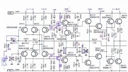
RA-971 DC circuit analysis
Ok, due to the absolute abundance of encouragement here, I will try another technical blurp - this time on on amp DC analysis.
Reading electronic schematics (and making some sense out of them) can be daunting to the untrained eye.
This is perhaps particularly true for the RA-971 schematic, which at first glance looks like someone just grabbed a handful of components and sprinkled them out over the page, somehow making a working amplifier.
This amp topology is called a ”Double Differential Input with Push-Pull VAS” stage – with the far easier acronym ”DDIwPPVAS”. Try saying that backwards after a few pints!
The beautiful idea behind this topology is that everything is symmetrical (even mirrored) in and around the audio signal path.
All things equal, this should provide a better audio performance, but in practice we shall see that it isn’t always so.
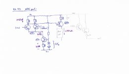
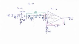
To get a better understanding it is a good thing to break down the schematic into its individual parts, blanking out other distracting bits.
In the attached pic I have only drawn the NPN half of the input and VAS stage. The PNP part is exactly the same – well that is, just sort of opposite, so to speak - oh, never mind.
There are three parts that work closely together here, a current source (CS), the input pair (LTP) and the upper Voltage Amplification Stage transistor (VAS).
Firstly, lets look at the CS that controls the DC current through the input stage.
It consists of two diodes, a transistor and a resistor. Let’s ignore base currents and assume that all diode Vd (and transistor base to emitter Vbe) voltage drops are 0.65V.
This means that the resulting voltage over the 220R resistor is forced to be (2*Vd – 1*Vbe) - or 0.65V.
Thus, this circuit produces a stable (0.65V/220R) = .003A – or 3mA which is pulled through the upper LTP.
Here, this current is shared equally between the two LTP transistors (if they are properly matched).
So the current through each 1k5 collector resistor is 1.5mA, leaving a voltage across it of 2.25Vdc.
This voltage drop is also present at the VAS transitor base, and subtracting its Vbe gives 1.4Vdc over the 365R resistor. Therefore, the resulting VAS stage current will be (1.4V/365R) = 4.4mA.
(With the original 100R in place it was (1.4V/100R) = 14mA, toasting the VAS transistors, because the voltage across them is (49V – 1.4V – 1.1V) = ~46V, dissipating (46V * 0.014A) = 0.65W in a TO-92 package. I measured temps over 72[FONT=Liberation Serif, serif]°[/FONT]C !)
So, breaking things down this way makes the circuit understanding and analysis just a matter of repeatedly applying good old Ohms law - well at least as for the DC behaviour of the amp.
No wizardry needed.
Ok, so why then is the resulting specs for the ”DDIwPPVAS” - with all its schematic symmetry beauty - not any better than a ”normal” single VAS amp topology. I guess that the answer lies in the difficulties of matching all the transistors (both for hFE and Vbe) – particularly between the NPN and PNP types. And even more so when it comes to mass production of these amps.
Ok, due to the absolute abundance of encouragement here, I will try another technical blurp - this time on on amp DC analysis.
Reading electronic schematics (and making some sense out of them) can be daunting to the untrained eye.
This is perhaps particularly true for the RA-971 schematic, which at first glance looks like someone just grabbed a handful of components and sprinkled them out over the page, somehow making a working amplifier.
This amp topology is called a ”Double Differential Input with Push-Pull VAS” stage – with the far easier acronym ”DDIwPPVAS”. Try saying that backwards after a few pints!
The beautiful idea behind this topology is that everything is symmetrical (even mirrored) in and around the audio signal path.
All things equal, this should provide a better audio performance, but in practice we shall see that it isn’t always so.
To get a better understanding it is a good thing to break down the schematic into its individual parts, blanking out other distracting bits.
In the attached pic I have only drawn the NPN half of the input and VAS stage. The PNP part is exactly the same – well that is, just sort of opposite, so to speak - oh, never mind.
There are three parts that work closely together here, a current source (CS), the input pair (LTP) and the upper Voltage Amplification Stage transistor (VAS).
Firstly, lets look at the CS that controls the DC current through the input stage.
It consists of two diodes, a transistor and a resistor. Let’s ignore base currents and assume that all diode Vd (and transistor base to emitter Vbe) voltage drops are 0.65V.
This means that the resulting voltage over the 220R resistor is forced to be (2*Vd – 1*Vbe) - or 0.65V.
Thus, this circuit produces a stable (0.65V/220R) = .003A – or 3mA which is pulled through the upper LTP.
Here, this current is shared equally between the two LTP transistors (if they are properly matched).
So the current through each 1k5 collector resistor is 1.5mA, leaving a voltage across it of 2.25Vdc.
This voltage drop is also present at the VAS transitor base, and subtracting its Vbe gives 1.4Vdc over the 365R resistor. Therefore, the resulting VAS stage current will be (1.4V/365R) = 4.4mA.
(With the original 100R in place it was (1.4V/100R) = 14mA, toasting the VAS transistors, because the voltage across them is (49V – 1.4V – 1.1V) = ~46V, dissipating (46V * 0.014A) = 0.65W in a TO-92 package. I measured temps over 72[FONT=Liberation Serif, serif]°[/FONT]C !)
So, breaking things down this way makes the circuit understanding and analysis just a matter of repeatedly applying good old Ohms law - well at least as for the DC behaviour of the amp.
No wizardry needed.
Ok, so why then is the resulting specs for the ”DDIwPPVAS” - with all its schematic symmetry beauty - not any better than a ”normal” single VAS amp topology. I guess that the answer lies in the difficulties of matching all the transistors (both for hFE and Vbe) – particularly between the NPN and PNP types. And even more so when it comes to mass production of these amps.
Attachments
Last edited:
Adcom? Isn't that based on a Nelson Pass design?
I would have thought that you'd need to get up very early in the morning to upgrade or improve a Pass amp.
And mornings are not my speciality....
But if anyone has got the schematic, I would like to have a look.
Per
I've shown you can fall out of bed at noon, stuff it full of caps, blow on it with a fan, and be listening to a 15W class A Pass mosfet amp in time for an early happy hour.
Summer / Consolation Amplifier: 1995 Adcom GFA-5200
Attached is the schematic for the Adcom GFA-5300. All I can tell is that the mosfets make it run, while the BJTs make it stop.
Attachments
Ok, due to the absolute abundance of encouragement here......
Hi there Per,
Thanks for your teachings about the finer art of how does an amp function 😀
I would like to comment but i do not have had any education in electronics so to not make an absolute idiot of myself i don't.
This doesn't mean that it is not appreciated 😉
Cheers, Paulus
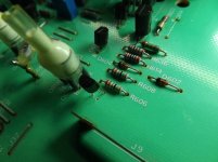
This RA-971 upgrade has been giving me a great deal more grief than usual. Mainly because of a string of my own stupid mistakes (reversing my CM1 and VAS3 NPN and PNP modules etc.) but once I removed, repaired and finally got the placements right, all looked just fine - for a while - until things suddenly started to drift up and away - and once again ended in blue smoke before any explanatory measurements could be done.
Aaaaargh!
I have now come to the conclusion that modules with tiny SOT-23 (max 300mW) transistors probably have no place in these high rail voltage amps.
At the least a significant design change of the current modules is needed.
These modules were designed so they could be easy direct drop-in replacements for the LTP collector resistors and the VAS transistors – without any need for cutting of pcb tracks, airwire components etc.
This works perfectly on the RA-930/931/01/04 etc. topologies, but on the double-differential design e.g of the RA-971, this is clearly not as straightforward.
But with two easy pcb track cuts and some 0.8mm hole drilling you can still put in emitter follower transistors before the two VAS trannies – which will greatly increase linearity and reduce LTP load and harmonic distortion. Unfortunately, this cutting and drilling will of course differ from one amp pcb layout to the next.
Anyway, I finally did it on the right channel of this RA-971. So I now not only have tamed the thermal issues and tidied up the looks of the inside amp, the THD was actually reduced from 0.0018% to 0.0010%.
The output offset was also reduced to less than +/-1mV by direct coupling the preamp to the power stage, which I could do because of the outstanding DC offset properties of the OPA2134.
Because, well if there is one major criticism of Rotel’s design – it would be that it appears as if each individual stage seems to have been developed and completed separately – and then it all was all put together as ”building blocks” on the final integrated amp pcb.
This means that each stage has its own input and output DC blocking, so you find double DC blocks between stages using electrolytic capacitors – where actually (ok well, now) none is actually needed.
So, the schematic of the improved amp is below with the changes highlighted in (a sort of) pink.
Things were nice and stable, bias setting easier, no trace of instability, THD excellent etc. There is only one electrolytic cap left in the channel, the feedback 220uF Panasonic FM.
But there was a problem.
The amp's upper -3dB frequency was suddenly only just over 40kHz. I will let the cunning hawk-eyes watching on this thread ping in with the where and why. It took me several hours of searching and experimentation before finally - the great smack hit the forehead. Duh!
Per
Attachments
Last edited:

I hope this basic explanation makes any sense. Otherwise, I intend to follow the advice of the great Tom Lehrer: ”If people can’t communicate – the very least they can do is to SHUT UP!”
Pithy advice that remains as needed now as when I first heard TL decades ago 😉
Great work as ever, Per.
Well, the cunning problem solutions to the upper 40kHz limit did not exactly flood in, so I will just explain what I did.
When something unexpected like this happens, it is generally good practice to re-trace your steps one by one, regardless of what you may or may not expect – you could have missed something.
And when the upper frequency range is suddenly drastically reduced, it has something to do with circuit changes in - or around capacitors.
1) So, moving from right to left on the schematic, I started from the output driver stage where I first replaced the 47R with 157R || 100n. Reverted back to 47R and measured – no change (as expected).
2) Then to the increase in VAS emitter resistors R621/623, briefly going back to 100R and measure – no change.
3) I also changed the bias circuit bypass C611 to a 1uF film capacitor, tried to parallel it with the original 10uF – measured, no change. 4) Same with undoing the changes in C609 and R629.
5) OK, so has the VAS output impedance then changed by introducing the emitter followers, interacting with the 220pF stability caps C613/615? Lifted these, measured – no cigar.
Which is fine as smoking is not good for you, but it left me scratching my thinning hair line - because then what?😕
I decided to re-draw part of the schematic. This shows some of the points I made before, that each stage of the amp seems to have been designed in isolation and everything then put together as "building blocks" on the pcb. Thus, there is double DC blocks between the stages.
First, consider the power amp stage (here drawn as a big opamp). Inside, I have only drawn the upper input LTP transistors. Each of these get a 1.6mA DC pulled through it by the current sources. If we assume that they are well matched and have a hFE of say 400 then for their service they will require a base current Ib of 1.6mA/400 = 0.004mA, or 4uA. This has to come from somewhere.
These DC current paths are indicated in red, the ”+” input get its through the 47k, the ”-” base from the 12k in the NFB circuit. This gives a voltage difference over the inputs of (47k-12k) * 4uA = 140mV which would give a significant amp output offset.
Fortunately it isn’t as bad as that because in the double differential topology the upper NPN LTP will pull its Ib whereas the lower PNP pair will source it – or rather supply the NPN’s. If they all are well matched.
In the early BJT opamp days it was repeatedly recommended that you should try to ensure that the amp inputs had the same dc resistance load.
But here, increasing the NFB 12k to 47k is not a good idea, as the resistor Johnson noise goes up.
Likewise, reducing the +input 47k to 12k would require a 4 times larger cap than the 4k7 to maintain the bass frequency response.
The 12k direct DC coupling I eventually chose between the pre- and the power amp stages is shown in green, not only gets rid of electrolytic caps and high ohmic resistors in the audio path, but also (almost) removes the amp output offset. Big smiles all around😀 – well, except for the 40kHz bandwidth issue🙁
And there it is – before your very eyes: The -3dB frequency point of a RC filter is (1 / 2π RC)
Which here gives (1 / 2π * 12k*330pF) = 40.2kHz Duh indeed!
Lifted the 330pF – and the bandwidth went to 440kHz.
This small input capacitor is so standard that it it is often simply overlooked. Its function is to shunt out any RF interference.
If you have ever played a high impedance pickup Fender over a guitar amp you will know what I am talking about. At least in central Europe, even in the deepest basement practice room you would often get friendly radio Moscow received, de-modulated and pounded out through the speaker.
За встречу (Za Vstrechu) !
(The band would even say "leave it on - sounds better than you playing" - cheeky b*stards!)
But between an integrated amp pre - and power stage this capacitor is not needed - and over the shoulder it went.
I guess it is time to pack the amp back together for a proper listening test......
Cheers,
Per
Attachments

RA-971 finished!
Well, after a first listening test where the amp sounded a bit (read: very) disappointing, I took it back to the workbench and found out that I had put in one of the new emitter followers the wrong way around.🙁
No excuse for that, although with all these mirrored NPN and PNP transistors there is definitely a great need to keep fully focused through the entire upgrade process.
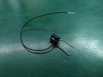
In the 971, I actually found placements for these EF trannies that enabled their collector pins get direct access to ground. But in other pcb layouts this may be difficult.
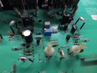
So, I would suggest lifting the centre pin and wire-wrap a length of wire to it, see pic.
This gives a degree of placement freedom, as you only need to find a pcb track leading to the VAS base (with some room above for the tranny), cut the track and drill two small holes for the EF's base and emitter (the right way around!). Then find a GND somewhere to solder the collector ww wire to. Add the 2k2 resistor between the VAS base and emitter - and Robert is your dad's brother.
I test these amps on a pair of Mission speakers, which I have found to be extremely dependent on the amp that drives them. Put a bland amp on and they will sound lazy and - well, bland.
The Rotel RA-971 AP Signature on the other hand suddenly brings the best out of them: commanding, detailed, precise, full soundstage etc. What a difference!
Ok, I will stop my ranting.
If any RA-971 owners here would like to try this upgrade, I will be here to help if you need it. It is definitely worth the effort!
Happy modding and keep safe in these strange times,
Per
Well, after a first listening test where the amp sounded a bit (read: very) disappointing, I took it back to the workbench and found out that I had put in one of the new emitter followers the wrong way around.🙁
No excuse for that, although with all these mirrored NPN and PNP transistors there is definitely a great need to keep fully focused through the entire upgrade process.
In the 971, I actually found placements for these EF trannies that enabled their collector pins get direct access to ground. But in other pcb layouts this may be difficult.
So, I would suggest lifting the centre pin and wire-wrap a length of wire to it, see pic.
This gives a degree of placement freedom, as you only need to find a pcb track leading to the VAS base (with some room above for the tranny), cut the track and drill two small holes for the EF's base and emitter (the right way around!). Then find a GND somewhere to solder the collector ww wire to. Add the 2k2 resistor between the VAS base and emitter - and Robert is your dad's brother.
I test these amps on a pair of Mission speakers, which I have found to be extremely dependent on the amp that drives them. Put a bland amp on and they will sound lazy and - well, bland.
The Rotel RA-971 AP Signature on the other hand suddenly brings the best out of them: commanding, detailed, precise, full soundstage etc. What a difference!
Ok, I will stop my ranting.
If any RA-971 owners here would like to try this upgrade, I will be here to help if you need it. It is definitely worth the effort!
Happy modding and keep safe in these strange times,
Per
Attachments

Last edited:
Hi there Per,
You did it, again!
If memory serves me well and reading #402 this would also be an upgrade for my 2 RB-991's?
That would be the cherry on the cake so to speak 😀
Cheers Paulus
You did it, again!
If memory serves me well and reading #402 this would also be an upgrade for my 2 RB-991's?
That would be the cherry on the cake so to speak 😀
Cheers Paulus
AngelIP I don't think the problems with your CM modules in the RA-971 are entirely down to the high rail voltages but because once you insert the CMs the VAS current becomes undefined. This is an old problem much discussed on this forum. Oddly enough if you just put a CM on one side only it should work fine. The collector resistors of the unmodified differential pair define the VAS current and the global feedback ensures that the differential pair with the CM folllows suit. Not my idea but lifted from the latest edition of Self's book. If you want to load both differential pairs with current mirrors then you have to use a few more components. There are many ways to do this and I have used but one in my "Mirror VAS" thread. You could probably add an extra transistor to your VAS circuit to implement this.
If memory serves me well and reading #402 this would also be an upgrade for my 2 RB-991's?
That would be the cherry on the cake so to speak 😀
Cheers Paulus
Hi Paulus,
Yes indeed, that was one of the reasons for practising this upgrade on the RA-971.
If you want, I can send you the wire-wrapped KSA992 and C1458's - you'll have to figure out where to place them, but I know that you are quite good at that.
Cheers,
Per
AngelIP I don't think the problems with your CM modules in the RA-971 are entirely down to the high rail voltages but because once you insert the CMs the VAS current becomes undefined.
Hi Chalky,
I think that you are absolutely right.
I made the modules for the single VAS RA-931 and it works superbly due to the nice stable current source for the Bias/VAS stage.
But in the RA-971 the VAS current is set by the +LTP transistor(s) collector voltage, and relinquishing that control by putting in a CM, the VAS stage current seemed to start drifting upwards and the module's small SOT-23 trannies soon decided to leave the Surface part of SMT for a more heavenly resting place.
It could also be due to that in the VAS3 module the EF emitter 2k2 resistor does not go directly to the rail, rather through the VAS emitter resistor - which I actually increased from 100R to 332R.
Maybe it's time for a VAS4 design?🙂
Per
Last edited:

Had a quick look and found the 2SB1275/2SD1918 and 2SA1552/2SC4027 smt ( SC63 ) pairs both of which dissipate between 1 and 15W depending on conditions. There may be better.
Hi Paulus,
Yes indeed, that was one of the reasons for practising this upgrade on the RA-971.
If you want, I can send you the wire-wrapped KSA992 and C1458's - you'll have to figure out where to place them, but I know that you are quite good at that.
Cheers,
Per
Hi there Per,
You make me a happy person 😀
Yes please, i would like to take you up on your offer.
I just send you email.
Cheers Paulus
You mean something like the idea below. You should be able to find higher dissipation smt transistors for the vas - the ones with tabs for soldering to an area of the pcb.
Yes, that is a clever design idea using a current mirror inside the VAS.
But my goal was to make a VAS module that would be a direct drop-in for the stock TO-126, so ideally a 3-port device (ok, the VAS3 is technically a 4-port, as it has a flying GND wire).
The above idea will make it a 5-port with the need for an extra current source to set the VAS current(s).
Actually, the last PNP emitter follower and its 330R resistor already acts as a 2mA current source for the middle NPN VAS,
which even with 80V rails is quite safe for the tiny VAS.
So it is almost always this last EF SOT-23 that is sent through hifi purgatory.
Indeed, a larger SMD transistor soldered on a reasonably sized copper area on the back of the module would be more resilient, but that won't change that the small module will heat up to excessive temperatures.
Thus it is this EF transistor's current (and thereby heat wattage) that needs to be controlled rather than the VAS - and you are right, it only needs one current source in the VAS/Bias string.
I was thinking at something like squeezing in a LM334?
Per
How about dispensing with the last pnp emitter follower and using a high dissipation smt device for the vas? Ok the distortion would probably be a tad higher but you've got a device that is better placed to cope with the dissipation. Or you could just use a high dissipation device for the last pnp emitter follower? As a general point I have found that gluing a small dip8 heatsink on top of sot-23 devces is quite effective at keeping the temperature down. Use the thermal adhesive for fixing leds to heatsinks.
Complementary differential IPS instability
Per,
Thank you for your comprehensive "research" how to improve these Rotels. I have been watching this for some time now.
The problems you have experienced with your current sources and stability have been described by Bob Cordell in his (highly recommended) book. And by D.Self as chalky mentioned.
"...
Complementary differential input stage with current mirror loads suffers quiescent bias instability...
... there is a current mirror on top driving the PNP-VAS transistor and another current mirror on the bottom
driving the NPN-VAS transistor.... The VAS quiescent current is indeterminate.
This is not a practical and reliable circuit. Some means must be introduced to
establish some reliability with the VAS bias current...."
Bob also shows a solutions for this:
"One approach to solving this problem is illustrated in Figure 7.10. First notice that
each current mirror has had a helper transistor added to it (Q13, Q14). This is little more
than an emitter follower that supplies the base current for the current mirror transistors,
rather than having it drained from the incoming current. This improves DC balance of the
current mirror and greatly decreases the influence of transistor beta on its operation..."
As I have a RB985 (5ch PWR-amp) myself I am especially interested in improving the complementary differential IPS type of circuits.
All these (bigger) Rotels have very similar circuitry, the main differences are the compensation schemes (at least for me).
BTW, how do you test for stability when you do changes in that area?
The RB985 comes already with some extra features the others don't have, which makes it an interesting modding object:
- Zobel-Element
- Output inductor
- IPS and VAS decoupled by RC
- DC servo (I think, need to confirm). OK, if this is a benefit...some people may disagree
Unfortunately mine is broken, one channel down and it looks like the parcel service has dropped it. Transformer is loose and humming.
When I find the time I will try to fix it. But that is a different story.
joe
BTW, how do you test for stability when you do changes in that area?
joe
By counting the blue smoke signals from the transistors😉
No, honestly, I always (or rather - should always) put a DC coupled scope on the outputs and observe it - keeping the fastest finger in the west on the power OFF button.
Often I also have at least one DMM on the VAS string to check that the voltages are roughly as expected.
When my hubris sometimes convince me not to bother - often putrid blue smoke ensues.
My goal is to make upgrade modules that contain all or most of the solution, so drilling and pcb trace cutting can be avoided or kept to a bare minimum.
This is what most modders (including myself) seem to be most uneasy with. We probably all want a safe way back to stock if/when things go awry.
Anyway Joe, thank you for your kind words.
Cheers,
Per
"One approach to solving this problem is illustrated in Figure 7.10. First notice that
each current mirror has had a helper transistor added to it (Q13, Q14). This is little more
than an emitter follower that supplies the base current for the current mirror transistors,
rather than having it drained from the incoming current. This improves DC balance of the
current mirror and greatly decreases the influence of transistor beta on its operation..."
joe
I don't have Cordell's book, could you perhaps scan that figure and PM me? Or, even better - point me to where I may find a copy of the book?
Cheers,
Per
- Home
- Amplifiers
- Solid State
- Improve a Rotel amp THD by 20dB!