I'm a little worried that R16 should be a "beefier" trimpot (Bourns 3296W 500mW specified). At mid-rotation, under full load conditions it will be maxed-out.
Looks pretty good -- will have to test for output impedance next:
An externally hosted image should be here but it was not working when we last tested it.
Hi, any pcb left for me? I want four pieces...Thanks in advance for the quick answer.
Regards,
Horia.
Regards,
Horia.
Only 6 PCB left.
Lordvader, I guest you're testing the circuit with a load attached. The tests voltages on this circuit depends on using the same very test load, in this case 22K. If you use a different value, you may get other results.
At the first look I think you have problem because you're testing this circuit in the wrong way. Shunt regulator can be confusing compare to a standard serie regulator.
R12 voltage. First this is the shunt current reading resistor. The total regulator current (LOAD + shunt, here current passing throught R12) is set by R16. IF THE SET CURRENT is too low for the load, the shunt regulator output will be ZERO... Hence the need to check the regulator with the same test resistance, or to know exactly what you're doing.
This regulator can supply a maximum of 125ma AND a minimum of 20ma. A shunt regulator regulate the output voltage by shorting to ground some of the source current, loading the voltage.
First you need to calculate (or test with a regulator serie supply) what will be the normal load current at your needed voltage, example 30ma. Then you add some shunt current, example 20ma. That gives a total of 50ma. So you need to adjust R16 in order to get this current. Turn R16 until the output HV increase, and that you start to have so current going throught R12, then set it for 20ma in R12.
Last edited:
I'm modifying one of the boards to use the DN2540 instead of the aux power source for the error amplifier.
Other voltages
pin 2 = 7V (fine)
pin 3 = 1.2V (wrong !!!)
Pins 2 and three are the input of a differential amplifier. They have to be the same when your regulator is at the correct output voltage. pin2 is the reference volatge, here 7V. Pin3 at 1.2 volt simply indicates that your output voltage is too low, probably because your cannot supply enough current, see before...Nothing wrong there.
pin 6 = 0.9V (correct for mostfet shunt) 0.9V indicates that the circuit is not working, again current to low.
pin 7 = 10.6V (correct) IC supply, correct.
Checking other voltages, the voltages immediately after T2 are way low. RAW DC coming in about 300V, but after T2 the voltages are 65V.
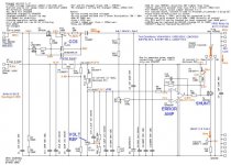
What should the initial position of R3 be ? The documentation has no mention of a default value ...R3 is simply a resistive voltage divider formed by R19+R18 and R13+R17 You can simply calculate the preset value by knowing that at the correct output voltage the output of this voltage divider has to be 7.0V. With the default values used on the schematic for R17-R19 the possible adjustable range is 230 to 470V as indicated on the notes. In equation 7V = Vset x (R17+R13)/(R18+R19+R17+R13) or 7V = Vset x (R13 + 4K7) / (304K7 + R13)
For example for a minimum of 230V, R13 = 0 (set to minimum) so 230V x (4K7/304K7) = 6.98V, very close to 7V... It works.
Again for this reg to work, you need a pcb input voltage higher than 20V than the value you want to set the reg to. For example for 230V at the output, you need at least 250V at the input.
IMPORTANT. There is a trade-off to do here. DON'T use an input voltage higher than needed, or you can exceed the power dissipation of the CCS. For example, you cannot use a 500V input voltage with a 230V output voltage at 50ma. That would mean that the CCS would have to drop 270V (500-230) and dissipate 13.5W (270V x 50ma). It would certainly get really hot and destroy.
So use an input voltage near the output you want. USE the proper power transformer.
Read all the notes on the schematic CAREFULLY. It explains everything you need to know about this board.
Hope it help.
SB
pin 2 = 7V (fine)
pin 3 = 1.2V (wrong !!!)
Pins 2 and three are the input of a differential amplifier. They have to be the same when your regulator is at the correct output voltage. pin2 is the reference volatge, here 7V. Pin3 at 1.2 volt simply indicates that your output voltage is too low, probably because your cannot supply enough current, see before...Nothing wrong there.
pin 6 = 0.9V (correct for mostfet shunt) 0.9V indicates that the circuit is not working, again current to low.
pin 7 = 10.6V (correct) IC supply, correct.
Checking other voltages, the voltages immediately after T2 are way low. RAW DC coming in about 300V, but after T2 the voltages are 65V.
What should the initial position of R3 be ? The documentation has no mention of a default value ...R3 is simply a resistive voltage divider formed by R19+R18 and R13+R17 You can simply calculate the preset value by knowing that at the correct output voltage the output of this voltage divider has to be 7.0V. With the default values used on the schematic for R17-R19 the possible adjustable range is 230 to 470V as indicated on the notes. In equation 7V = Vset x (R17+R13)/(R18+R19+R17+R13) or 7V = Vset x (R13 + 4K7) / (304K7 + R13)
For example for a minimum of 230V, R13 = 0 (set to minimum) so 230V x (4K7/304K7) = 6.98V, very close to 7V... It works.
Again for this reg to work, you need a pcb input voltage higher than 20V than the value you want to set the reg to. For example for 230V at the output, you need at least 250V at the input.
IMPORTANT. There is a trade-off to do here. DON'T use an input voltage higher than needed, or you can exceed the power dissipation of the CCS. For example, you cannot use a 500V input voltage with a 230V output voltage at 50ma. That would mean that the CCS would have to drop 270V (500-230) and dissipate 13.5W (270V x 50ma). It would certainly get really hot and destroy.
So use an input voltage near the output you want. USE the proper power transformer.
Read all the notes on the schematic CAREFULLY. It explains everything you need to know about this board.
Hope it help.
SB
Attachments
Last edited:
Thanks for getting back to me.
I should have some spare time over the weekend to restest some things.
I did my testing with a 2.8K resistor, to simulate ~210V, @ 78ma.
I should have some spare time over the weekend to restest some things.
I did my testing with a 2.8K resistor, to simulate ~210V, @ 78ma.
This is what I was thinking of -- it can be found in Supertex application note AN-D30.
An externally hosted image should be here but it was not working when we last tested it.
Algar_emi,
has anybody built a higher voltage version of this design to provide 600v regulated output at 50-60 mA?
What component(s) value/tolerances would have to change to accommodate the higher voltage(s)?
TYVM,
has anybody built a higher voltage version of this design to provide 600v regulated output at 50-60 mA?
What component(s) value/tolerances would have to change to accommodate the higher voltage(s)?
TYVM,
Are you going to do another Group Buy?
If you do another Group Buy for these HV Shunt Regulator PCB, count me in for
at least four. Let us know. Take care.
If you do another Group Buy for these HV Shunt Regulator PCB, count me in for
at least four. Let us know. Take care.
Two HPHV PCBs for sale
I have two unused PCBs left over from my projects. Please PM if interested in them. One of the boards has been trimmed on all four sides, so is smaller than the other. If you think you can live with this, I can let the boards go for $20 for both. I can throw in all the resistors necessary to build two boards, and some other odds and ends.
I think this is better than putting the PCBs in the dumpster: they cost $25 each, so they were not cheap. 😀
I have two unused PCBs left over from my projects.
The two boards have been sold.
Two HPHV shunt regulators for sale
I now have two built-up HPHV shunt regulators for anyone who wants them. I have discovered, belatedly, that these regs are not suitable for my power amps (Vacuum State DPA-300B) because the amps draw more power than these regs can handle. I have therefore reverted to using the original Allen Wright-designed Superregs.
One of the regs is working, the other not. Unbeknownst to me, the regs were running incredibly hot. The failed board's shunt heatsink has turned from black to gold, so hot did it get. It's possible that all that is wrong with the failed board is that the shunt MOSFET has died. But it's also possible that when the shunt died it took the CCS with it.
So, one working board and one dead board. Anyone interested? PM me and we can agree on a low, low price for the good board with the dead board thrown in for free.
Yes, I have them working perfectly from the beginning...
Just follow the instructions and you'll be happy!
Just follow the instructions and you'll be happy!
Yes, I have them working perfectly from the beginning...
Just follow the instructions and you'll be happy!
Did you lower the values of R11 and R21 or make any other changes ?
Mine is now during testing decreasing the current through shunt (measured on point I) while the Vreg ramps up. If the Vreg is on target, the shunt current is zero. Sometimes the shunt current stays zero and other times the process repeats time after time from max current to zero. I also tried with LF351, same process.
- Home
- Group Buys
- HV Shunt Regulator PCB