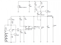
Hi againOn the contrary, in this version of GLED431 transistors play an essential role in the operation of the reference, they are selected to obtain the lowest possible noise and impedance which are much lower if we compare with LM329. There are two improved GLED431 versions in this regulator(s), for 6.8V and 9V.
Normally this low noise ref affects on performance of the regulator and the final impact on the sound.
All the best
Igor
Thanks for the detailed replies and apologies if I'm missing something - given that the reference is feeding a 500 ohm / 100uF RC filter and then on from that the opamp input, is low impedance a requirement for the reference in this application?
In any case, really appreciate the updates! I am putting together a monstre board and your experience is very encouraging - will integrate a reg design into the pcb as a result.
Best
Cv
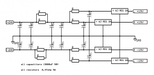
Hello grunf, I missed the regulator you use, any schematic for it?
Actually I am going to try a LC configuration, but I am looking for something less volumen consuming.
Despite of that I like the sound the monster offers, even if I use the classical configuration by Hiraga with low current around 0.6 A.
Actually I am going to try a LC configuration, but I am looking for something less volumen consuming.
Despite of that I like the sound the monster offers, even if I use the classical configuration by Hiraga with low current around 0.6 A.
Yes, low impedance and low noise is a requirement for the reference in this application and RC filter 500R/100uF can go to 10K/100uF for jfet op.ampHi again
Thanks for the detailed replies and apologies if I'm missing something - given that the reference is feeding a 500 ohm / 100uF RC filter and then on from that the opamp input, is low impedance a requirement for the reference in this application?
In any case, really appreciate the updates! I am putting together a monstre board and your experience is very encouraging - will integrate a reg design into the pcb as a result.
Best
Cv
https://refsnregs.waltjung.org/An_Improved_Reference_Filter_for_Audio_Regulators.pdf
Best
Igor
Hi HelmutHolzHello grunf, I missed the regulator you use, any schematic for it?
Actually I am going to try a LC configuration, but I am looking for something less volumen consuming.
Despite of that I like the sound the monster offers, even if I use the classical configuration by Hiraga with low current around 0.6 A.
I can't find the right link to my post where I posted the first version of the regulator so I'll put the schematic back on.
Now this version is quite improved but so far I am not allowed to publish details, CCSs are now with depletion mosfets and references have been improved by Mr. Walt Jung.
So far I have tried Le Monstre and 20W A class from Hiraga on these regulators, I still have to try JLH69 and somewhere I have a PCB with parts for Aleph 3 which I could also try with these regulators.
Le Monstre literally surprised me with the sound with these regulators, a really huge improvement, and most importantly regulators doesn't take up much space and they are relatively efficient with a voltage drop of around 4V.
Best
Igor
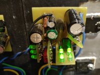
Attachments

check out this thread:It has nowadays become a matter of availability.
The common-emitter predriver is an important feature, but it is much more difficult to implement properly than the Darlington pair.
To solve the NPN-PNP mismatch and unavailability problem, I would consider the circlotron option.
I would stick to a big nonmetallic carbon (based) resistor.
https://www.diyaudio.com/community/threads/i-call-it-infinitron.270239/
Hi all,
I start building Hiraga 8w for first time using original schematic
My problem is I have brought wrong transistor version 😔
1st scenario
Input SK170-J74 BL
•SC1890-SA893
SB716-SD756
SD844-SB754
Not work
2nd scenario ( #117 by lineup low budget)
Input SK170-J74 BL
BC550-BC560 B
BD139-BD140
TIP41c-TIP42c / C5200-A1943
not work too 😔
my xFormer 12-0-12 with 12x1.4 = 16v after rectifier
I hope anyone can help me suggestions scenario using my existing transistor 🙏
Best regards
Rubah ganteng
The big problem is R5 and R6. This varies according to the transconductance of the input FETs. And in the original description Hiraga says you have to change this if you want to change the bias.
- Not work: when the current is too low then . . .increase the pair. The bias voltage of the output increases.
And it varies according to the resistance of the source of the input.
The output pair is just a follower, but a smart one.
in my opinion, if you take a pot for R5 and R6 then it can be done quickly, after solder in real resistances. Next tailor th the source resistors.
How? this is explained in the F5 manual, how to set up.
Note, I think it is important to have the same drain resistances R5/R6. I had 1k1 and 1k2, this differed on the voltage of the supply.
Attachments
transistor not fil hot and can't setting dcoHow does it not work?
i trying follow this guide
https://www.diyaudio.com/community/threads/hiraga-le-monstre.5462/post-1549714
Attachments

Last edited:
Indeed, if output idle current is too low (measured across 1 ohm resistor) then increase the values of the drain resistor, it depends on the real Idss and also but less on real Vb (I had 14 volts. Now I have 12 volts sound is less.) And I like almost > 1 amp best.
- I tried various values and did not use a potmeter myself - and I even bought the whole kit originally from the shop of Hiraga . . . so no new problems see the light, my Idss was slightly different from published.
Personally I would not change the source resistors. Several people have done just that. The original has 100 ohm pot. To set the DC out.
Last edited:
i try tonigh R3 260 and R4 300 without trimport 100Indeed, if output idle current is too low (measured across 1 ohm resistor) then increase the values of the drain resistor, it depends on the real Idss and also but less on real Vb (I had 14 volts. Now I have 12 volts sound is less.) And I like almost > 1 amp best.
- I tried various values and did not use a potmeter myself - and I even bought the whole kit originally from the shop of Hiraga . . . so no new problems see the light, my Idss was slightly different from published.
Personally I would not change the source resistors. Several people have done just that. The original has 100 ohm pot. To set the DC out.
View attachment 1073392
Note that with these values of R3 R4 then the curreint of the input is dramatically lower. It will require higher R5 R6. They are there only because many of the newer lots of the fets have a highr Idss than the 'Y' version. [some may even be fake, and really high]
I showed the diagram in post #2,148 only because quick find on computer, to be able to talk about the specific resistors, but this is from someone who 'designed' 2N3055 output in a sim that reflected one specific example of values.
- in my opinion, the input config. however should stick close to the original. [as long as the version is similar].
By disconnecting the output Q3 Q4 bases, then it might be easy to see: the voltage across the R4 R5 should be: 0,6 volt for the base + 0,8 V - what I have - for the current across the 1 ohm. So around 1,4V. If not change values untill you get there!
Hiraga's text:
One should not lose sight of the fact that the 8W functions in class A. The quiescent current therefore has a prime importance. Its value should not be too low otherwise the amplifier will pass into class AB on strong signals, nor too high because it would impose too great a dissipation on the power transistors which, in addition to the fact of limiting their lifespan, can lead to thermal runaway. Indeed, the characteristics of the power transistors are related to the temperature of the junctions and beyond a certain threshold there is runaway, that is to say the more the temperature rises the more the current increases. The optimal value lies between 0.5 and 0.6A.To measure the quiescent current, it is sufficient to measure the voltage across the 1 ohm 5W resistors. The voltage must therefore be between 500mV and 600mV. After sorting the batches of transistors, 2SD844/2SB754 on the one hand and 2SB716/2SD756 on the other, one can be placed in non-optimal operating conditions from the point of view of quiescent current. The remedy is extremely simple. If the quiescent current is too high, it is enough to decrease the bias resistors of 2SB716 and 2SD756 transistors, whose initial value is 1 kohm. These resistors coming from the bases of the transistors determine their point of operation and consequently the collector current, on which depends the quiescent current. In general, it is enough to change from 1 kohm to 910 ohm for the quiescent current to take the correct value again.
Last edited:
thanks u for your advice.Note that with these values of R3 R4 then the curreint of the input is dramatically lower. It will require higher R5 R6. They are there only because many of the newer lots of the fets have a highr Idss than the 'Y' version. [some may even be fake, and really high]
I showed the diagram in post #2,148 only because quick find on computer, to be able to talk about the specific resistors, but this is from someone who 'designed' 2N3055 output in a sim that reflected one specific example of values.
- in my opinion, the input config. however should stick close to the original. [as long as the version is similar].
By disconnecting the output Q3 Q4 bases, then it might be easy to see: the voltage across the R4 R5 should be: 0,6 volt for the base + 0,8 V for the current across the 1 ohm. So around 1,4V. If not change values untill you get there!
The output is not a follower............
The output pair is just a follower, but a smart one.
...........
It is a current mirror together with with bipolar transistors from drain of input transistors and with a gain of 1000.
The output pair is a Sziklai (inverted Darlington) configuration and the gain is about 8 times for a load of 8 ohms.
The gain from b1 node (or b2 node) to output node is 2RL/R18 (or 2RL/R19) = 16. The 2 times number comes from the push pull configuration. However, the current gain from the nodes b1 or b2 to the output is the two beta's multiplied and are more than 10000 times.
The gain (open loop) from the input to b1 (or b2) is just above 8 times, dependent of the IDSS and transconductance of the JFETs. The total open loop gain is about 140 times, so the feedback value is quite low, resulting in a very high output impedance (more than 1 ohm) and high distortion.
If JFETs with higher IDSS are chosen, R7 and R8 must be reduced accordingly if one wishes to have a bias current of the output at about 0.5 A.
Simulations are not more accurate than the models, but the results presented above is in full conformance with the calculated values.
(I have not Spice-models of 2SD844 and 2SB754, as used by Hiraga.)
Attachments

Last edited:
Hi all,
Would you guys please let me know what is the Le Monstre input impedance?
Also, what should be a good output impedance from a tube preamplifier to play with Le Monstre?
Tks
Nilton
Would you guys please let me know what is the Le Monstre input impedance?
Also, what should be a good output impedance from a tube preamplifier to play with Le Monstre?
Tks
Nilton
Can you share the pcb too?Hi HelmutHolz
I can't find the right link to my post where I posted the first version of the regulator so I'll put the schematic back on.
Now this version is quite improved but so far I am not allowed to publish details, CCSs are now with depletion mosfets and references have been improved by Mr. Walt Jung.
So far I have tried Le Monstre and 20W A class from Hiraga on these regulators, I still have to try JLH69 and somewhere I have a PCB with parts for Aleph 3 which I could also try with these regulators.
Le Monstre literally surprised me with the sound with these regulators, a really huge improvement, and most importantly regulators doesn't take up much space and they are relatively efficient with a voltage drop of around 4V.
Best
Igor
- Home
- Amplifiers
- Solid State
- Hiraga "Le Monstre"