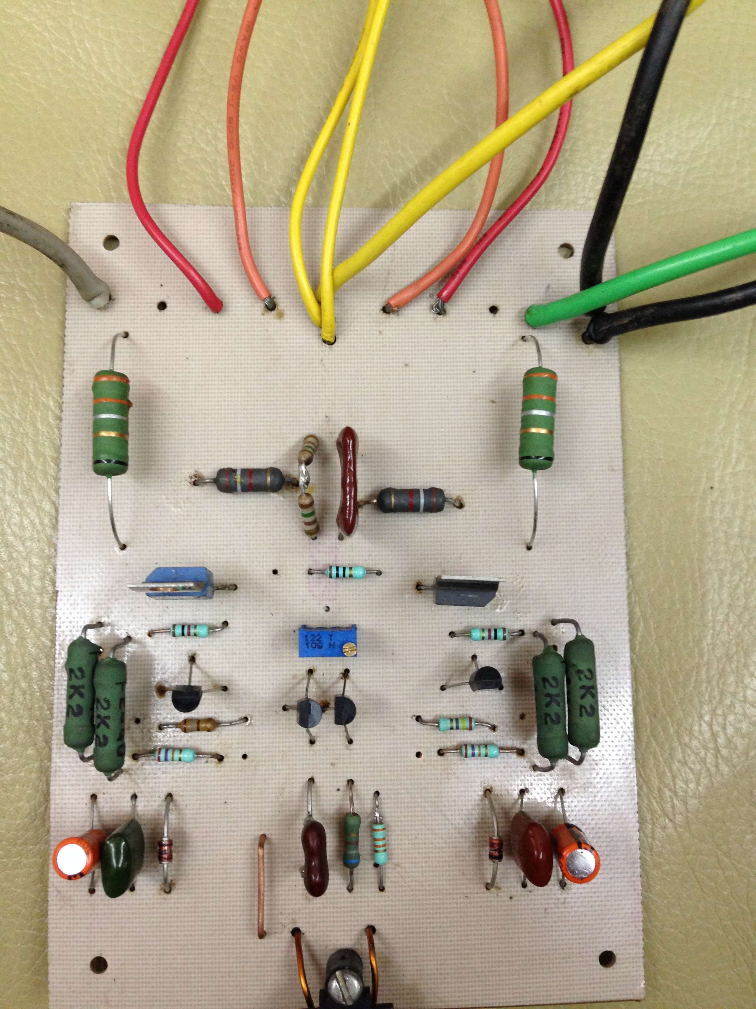
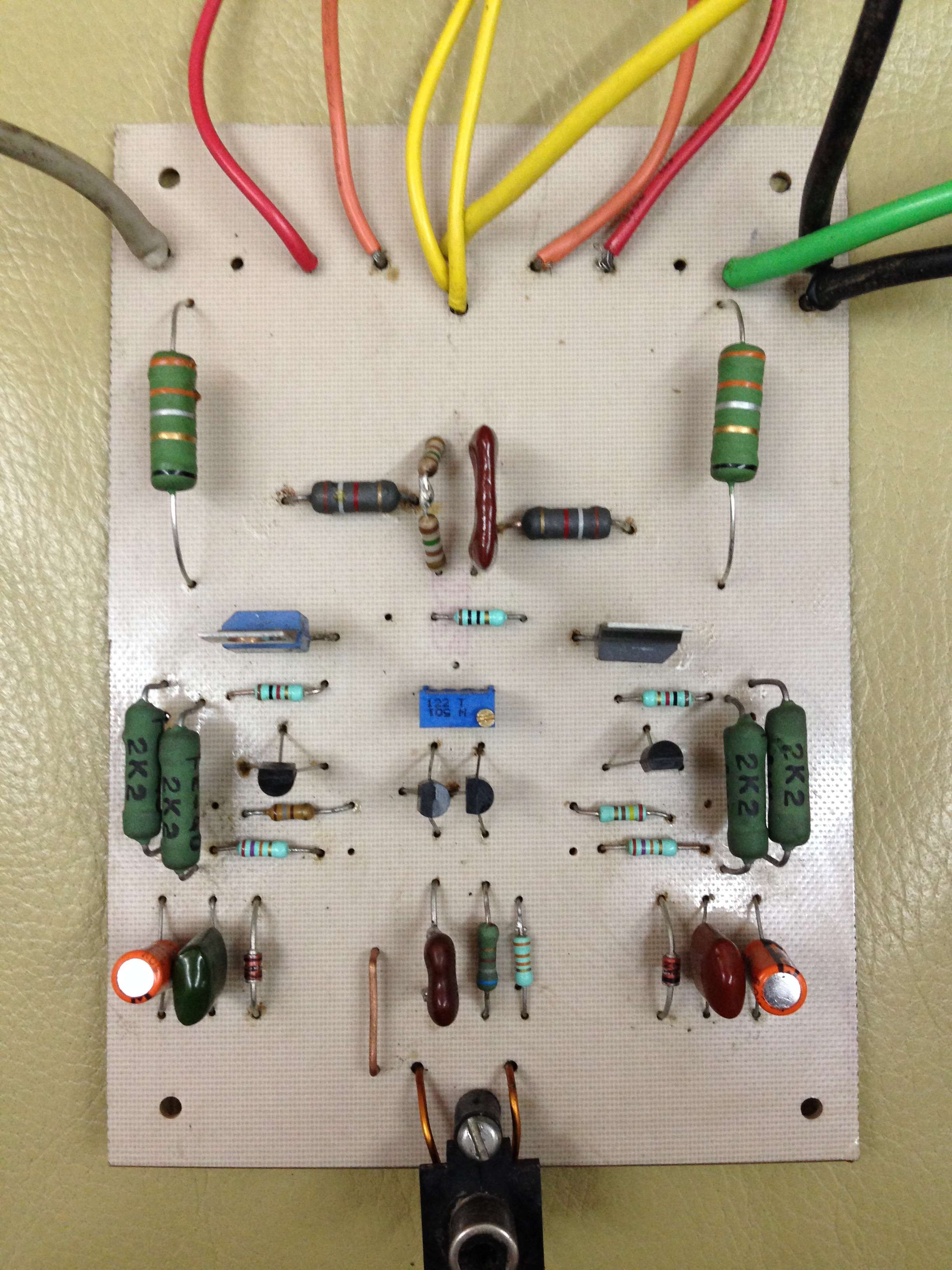
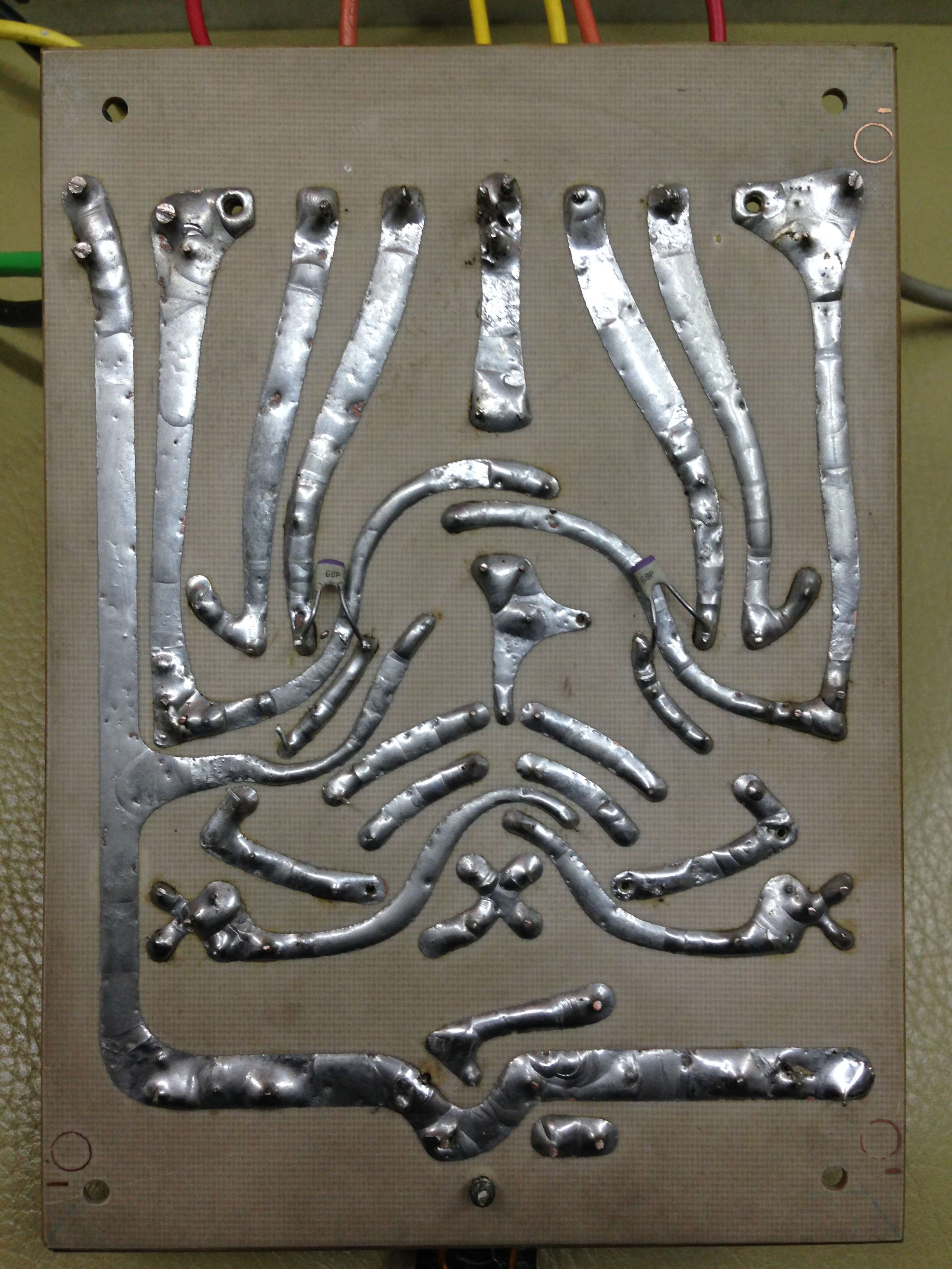
I'm sorry, I only speak in Portuguese, I'm using google translator. Someone could help me adjust the bias of my Hiraga, between base and emitter is with 12.5volts offset 4mv, thank you all from the forum. Silvestre Moraes
https://web.whatsapp.com/504b0b1b-518d-4f5c-b4ad-47b521c8b60a[/IMG]
blob:WhatsApp Web
blob:WhatsApp Web
https://web.whatsapp.com/504b0b1b-518d-4f5c-b4ad-47b521c8b60a[/IMG]
blob:WhatsApp Web
blob:WhatsApp Web
I need to adjust the voltage between base and emitter that is at 12.5 Volts. Anyone know how many mv would be?
I was able to adjust to 0.4 mv on the output.
See the pictures bellow.
WhatsApp Image 2019-05-21 at 20.16.22.jpeg - Google Drive
I was able to adjust to 0.4 mv on the output.
See the pictures bellow.
WhatsApp Image 2019-05-21 at 20.16.22.jpeg - Google Drive
Last edited:
in fact,you can adjust the bias uniquely with the two resistor 1.8k between the bases of the output transistors .
the potentiometer (500r or 1000r) is for adjust the offset
the potentiometer (500r or 1000r) is for adjust the offset
I need to adjust the voltage between base and emitter that is at 12.5 Volts. Anyone know how many mv would be?
I was able to adjust to 0.4 mv on the output.
See the pictures bellow.
I was able to adjust to 0.4 mv on the output.
See the pictures bellow.
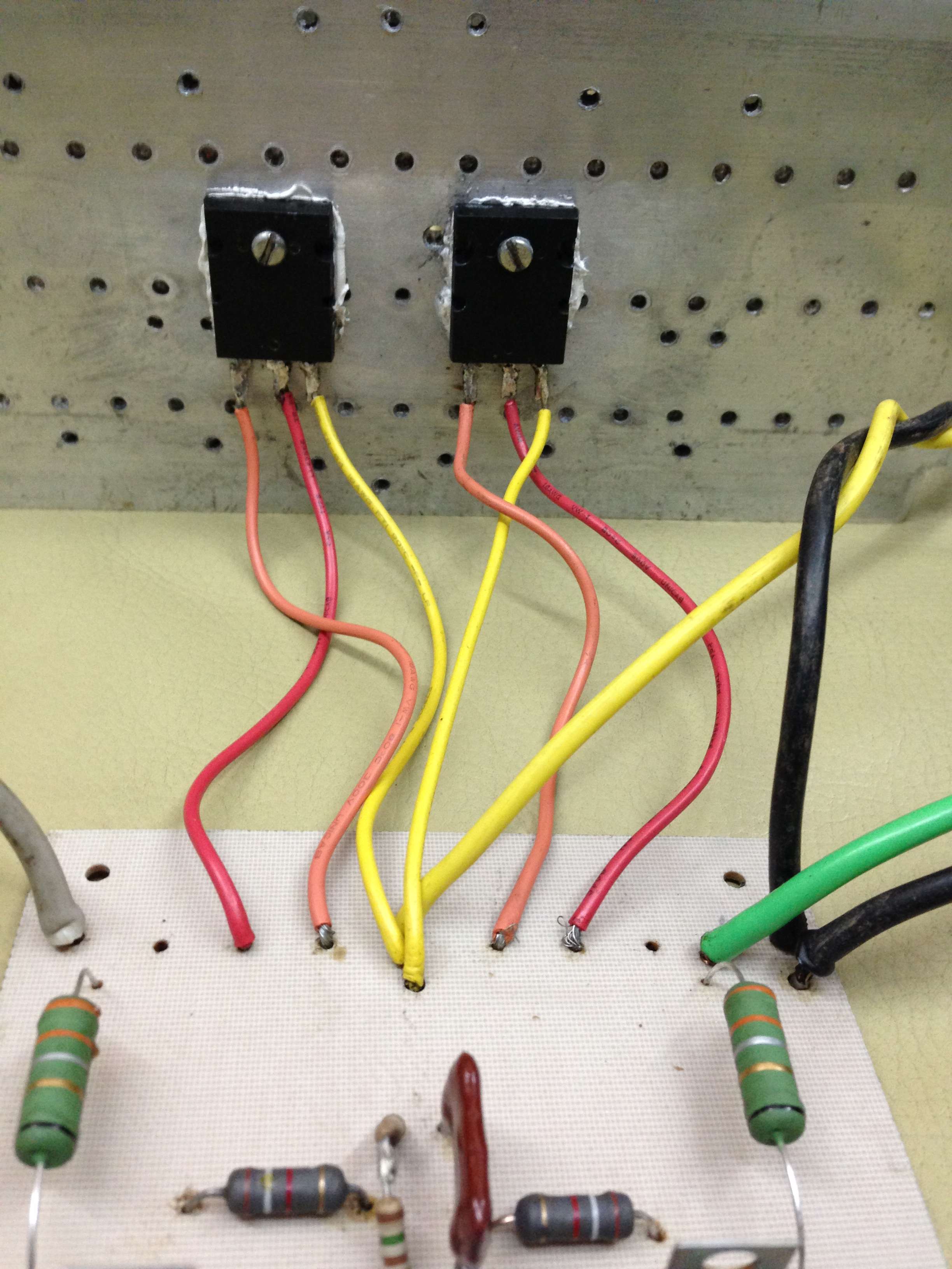
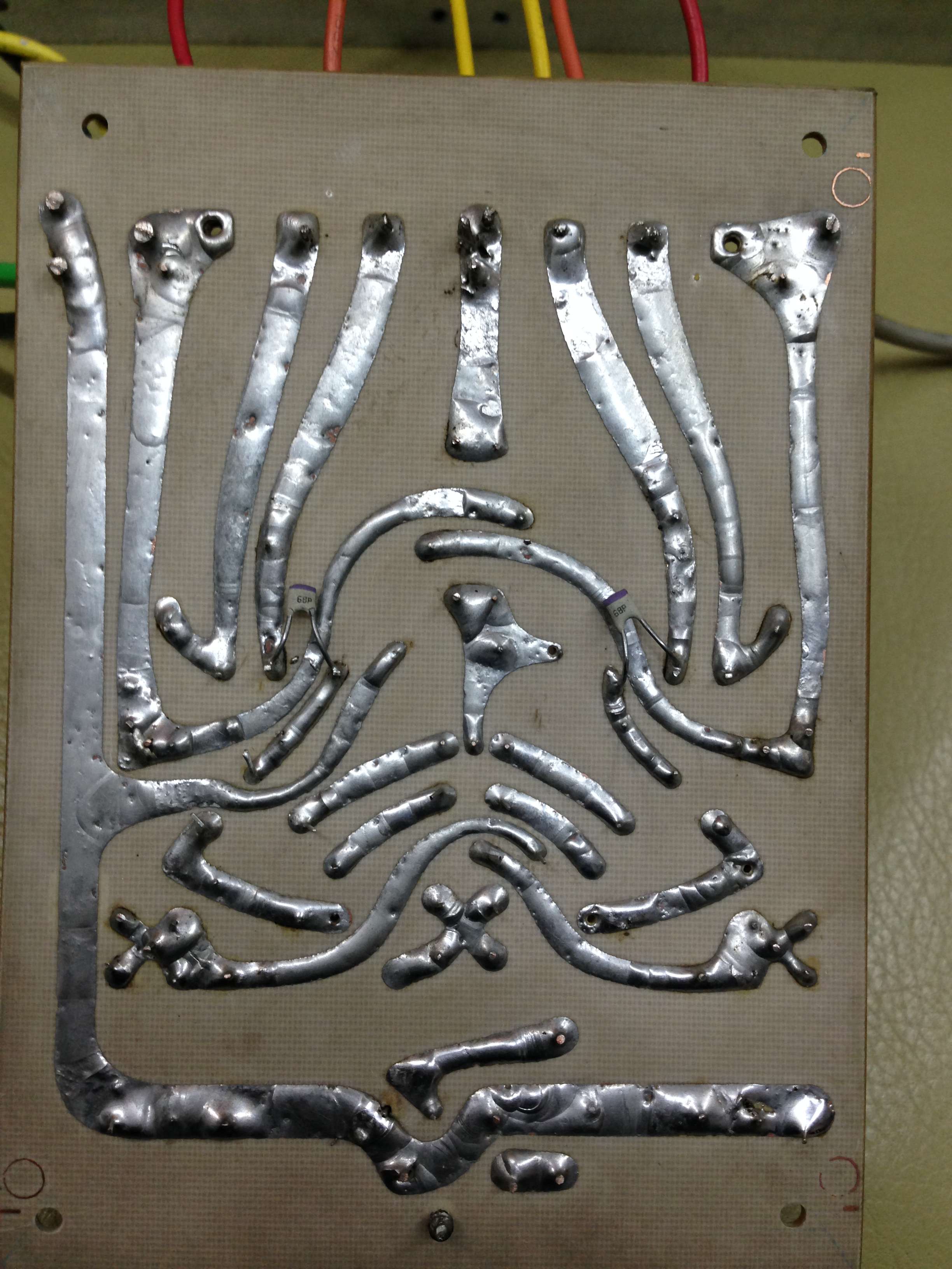
Some critisism: sloppy (bad) soldering. At least that is what it looks like.
I can see many wires not immersed like a liquid in solder. So there must be a bad contact.
The components have not been cleaned or have been resoldered many timesand the result is connections that are prone to decay, getting worse, for example when warming up, the sound changes or cracks are heard.
I had the same bad style (if it works it works?) and used 'modern' high temperature solder, but very hard to work with.
I since a few years use SAVBIT, expensive but the result is stable now.
i'm ok with Triode_Al ,you have to redo your solders.
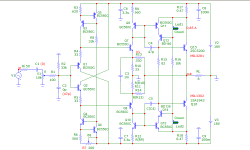
"30-0-30vdc it's too high .
this amp (with its original components) is very very sensitive to its supply voltage.
there you are closer to 30w.
the 20w must remain in the band of 18 / 23vdc, (23vdc max) charging.
if you can, try a variac or bucking transformer to lower the voltage on the primary and therefore the secondary.
if that's what I think, you'll be able to set your offset to almost zero with the right supply voltage.
I reviewed a real 20w from "La Maison de l' Audiophile"
which is over thirty years old.
because of the increase in the mains voltage, it was completely out of order.
I made him the complete power supply, added a bucking transform then changed the resistance of polarization and now, he left for thirty years of good and loyal services.
the most important with this amp is the power, you really have to do it properly and do not take too much freedom with the original plans.
Apart from supply voltage, you may know that the 13V is controlled by the RD13 zener diodes, which logically are 13V types. Equivalents are listed in supplier catalogues but they are unusual stock items and may be difficult to buy locally.
It's possible to select 13V zeners at the high or low end of their manufacturing tolerance there but you could try placing a common 1N4148 diode in series with a 12V zener in either location but in reverse polarity to it. This will bump the voltage up by 0.7V and may be enough to trim either the upper or lower zener voltage and shift the DC offset. However, I think the better way may be to adjust the emitter resistors in the input transistor pair. These are already offset in value (210Ω v 240Ω), which suggests there was a good reason for it. Much of it has to do with differences between the NPN/PNP input transistors which cause the offset.
In reality, there is no point in trimming to any closer than about 30 mV offset. It just appeals to our sense of precision to have 0 mV offset, just like we imagine symmetrical circuits to be better than asymmetrical 😉
Last edited:
that's why I asked him to give a try with a variac or a bucking transformer.
this zener is a function of the supply voltage.
this zener is a function of the supply voltage.
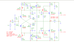
Driver and Power transistors in Hiraga super class A
Hi, I am building the Hiraga super class A based on the schematic posted in the DIY Audio Projects many years ago. I need to say that I am not very experienced with analoge designs. Anyway, I have ended up with driver transistors MJE 15030/MJE15031 and Power transistors SA1943/SC5200. When studying these stages it seems to me that this actually are two Sziklai pairs. When reading about Sziklai pairs on the net, it appears to be a common understanding that it is important that the two transistors in the pair should be complementary and closely matched. I am not sure that one can claim that the MJE15031 is complementary to the SC5200, nor the MJE15030 to the SA1943. Does anyone have a comment to this and why didn't Hiraga in the original design use complementary transactions both in the driver and the output stage? Can the SA1943 be used to replace the MJE15031 and vice versa with SC5200 for MJE15030?
Hi, I am building the Hiraga super class A based on the schematic posted in the DIY Audio Projects many years ago. I need to say that I am not very experienced with analoge designs. Anyway, I have ended up with driver transistors MJE 15030/MJE15031 and Power transistors SA1943/SC5200. When studying these stages it seems to me that this actually are two Sziklai pairs. When reading about Sziklai pairs on the net, it appears to be a common understanding that it is important that the two transistors in the pair should be complementary and closely matched. I am not sure that one can claim that the MJE15031 is complementary to the SC5200, nor the MJE15030 to the SA1943. Does anyone have a comment to this and why didn't Hiraga in the original design use complementary transactions both in the driver and the output stage? Can the SA1943 be used to replace the MJE15031 and vice versa with SC5200 for MJE15030?
Sorry, I will rephrase:
- The last stage in the Hiraga construction is known as a Sziklai configuration I think (Sziklai pair - Wikipedia). The NPN and PNP transistors in the pair should be complementary according to articles I have seen.
- Many people building the Hiraga amp are using the MJE15030/MJE15031 and SA1943/SC5200 transistors in the last stage.
- The question is: Are MJE 15030 complementary to SA1943 and MJE15031 complementary to SC5200 which the Sziklai pair supposely requires? More clear now?
Two remarks: a TL431 can be used to creat a great 13V source.
Secind, the "complementarity" has more to do woth the sort of matching of the high frequency capabilities, between the driver and output. That is different from the matching based of Hfe of the two outputs or drivers. The Darlingnot is determined by the driver if I understand correctly.
Secind, the "complementarity" has more to do woth the sort of matching of the high frequency capabilities, between the driver and output. That is different from the matching based of Hfe of the two outputs or drivers. The Darlingnot is determined by the driver if I understand correctly.
Attachments
Last edited:
Do I see 100% feedback? You will never get the 'signature' harmonics structure that Jean Hiraga designined in that way.
Is Hiragi's amplifier without feedback? The circuit is improved and only, the depth of feedback is increased while maintaining the structure of the amplifier.
Is Hiraga's amplifier without feedback? The circuit is improved and only, the depth of feedback is increased while maintaining the structure of the amplifier.
I read the schema wrong, you have 330 ohms/30 ohms in a Nelson Pass style feedback in the schema at the right.
- Home
- Amplifiers
- Solid State
- Hiraga 20W class A