Thanks, but that doesn't help as it's not in English.There is a little information about Jean Hiraga's Super Class A 20W & 30W Amplifiers. The 30W version has very very good sound, but I want to build 20W version.
I have been looking around for explanation, but I have no luck.
Thanks, but that doesn't help as it's not in English.
I have been looking around for explanation, but I have no luck.
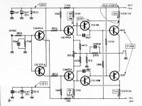
Hiraga's 20W or 30W need big power supply. Exist 2 version of 20W: 1979 and 1985. In version of 1979 in power supply used filter 0,36F (CRC 1:2, 60000 uF + 1 om (30W)+ 120000 uF per shoulder). In 1985 has been made new version of 20W and 30W with filter 1,456F (CRC 68000uF+0,22 om (25W)+2x0,33F per shoulder).
I builded Hiraga's 20W (1979) and 30W (1985) Amplifiers (the sound of 30W much better, than old 20W), now I building 20W (1985) (maybe will be better).
Last edited:
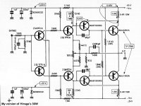
Warning - original schematic has mistake, "bottom" stabilitron must be mirrored (fixed in schematic in "my version"). 🙂Thanks, but that doesn't help as it's not in English.
I have been looking around for explanation, but I have no luck.
Old 20W version: http://sound.au.com/tcaas/hiraga1.htm
Attachments
Last edited:
Thank you very much, I have to read it.Warning - original schematic has mistake, "bottom" stabilitron must be mirrored (fixed in schematic in "my version"). 🙂
Old 20W version: The Class-A Amplifier Site - Hiraga 20W Class-A
Alan
Thank you very much, I have to read it.
Alan
Now I building 20W version (1985), because very interesting: what's better 20W or 30W.🙂
Attachments
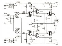
Now I building 20W version (1985), because very interesting: what's better 20W or 30W.🙂
It's a little late for me on the first round. I already bought a 30VAC 30VAC 625VA, big chassis with 300W heat sink on each side. Boards at the final stage of layout and parts ordered. But I am definitely interested in trying it out in the second round.
I am doing 3EF, 5 stages with 200mA per stage. So I am going to get 8W of pure Class A and 100W Class AB into 4 ohm with my amp.
I also just bought two of the 24V 15A switching power supply. I am planning on adjust the voltage down to say 22V and run +/-22V with over 300mA idle current per stage. Then I should get at least 18W of class A and about 50W Class AB.
Last edited:
It's a little late for me on the first round. I already bought a 30VAC 30VAC 625VA, big chassis with 300W heat sink on each side. Boards at the final stage of layout and parts ordered. But I am definitely interested in trying it out in the second round.
I am doing 3EF, 5 stages with 200mA per stage. So I am going to get 8W of pure Class A and 100W Class AB into 4 ohm with my amp.
I also just bought two of the 24V 15A switching power supply. I am planning on adjust the voltage down to say 22V and run +/-22V with over 300mA idle current per stage. Then I should get at least 18W of class A and about 50W Class AB.
What's mean "3EF" - it's amplifier?🙂
EF = Emitter Follower.
3EF = three EF pairs used in series as an output stage.
Sometimes referred as triple EF and consisting of pre-driver, driver and output devices.
This is different from a 3pair output stage which is formed from transistors in parallel.
3EF = three EF pairs used in series as an output stage.
Sometimes referred as triple EF and consisting of pre-driver, driver and output devices.
This is different from a 3pair output stage which is formed from transistors in parallel.
EF = Emitter Follower.
3EF = three EF pairs used in series as an output stage.
Sometimes referred as triple EF and consisting of pre-driver, driver and output devices.
This is different from a 3pair output stage which is formed from transistors in parallel.
Thank you for the info, because I don't quite understand the abbreviations in English.🙂
I read the article you gave, it's interesting. Is that a translation from another language? I find it hard to understand at times. But I get the idea.Thank you for the info, because I don't quite understand the abbreviations in English.🙂
It's something new that the distortion characteristics of the amp that can change the amplitude of the harmonics of the instruments and change the sound. So it's not about how low the distortion, it's the characteristics of the amp.
But the questions are:
1) What make this design better? Is the % of distortion is same in the entire audio frequency?
2) Any information on the on the theory of the composite output power transistor stage. The author only said it is equivalent to Ultralinear tap of the tube output stage.
Thanks
It would be very nice if the sound quality is determined only by the THD.I read the article you gave, it's interesting. Is that a translation from another language? I find it hard to understand at times. But I get the idea.
It's something new that the distortion characteristics of the amp that can change the amplitude of the harmonics of the instruments and change the sound. So it's not about how low the distortion, it's the characteristics of the amp.
But the questions are:
1) What make this design better? Is the % of distortion is same in the entire audio frequency?
2) Any information on the on the theory of the composite output power transistor stage. The author only said it is equivalent to Ultralinear tap of the tube output stage.
Thanks

I almost completed the 20W (1985) version, will soon learn that it is better to sound: 20W or 30W. 🙂
Last edited:
Hi
I am doing some analysis on my own. Here is my educated guess.....emphasize GUESS!!!
1) OPS is Q2 and Q3 forms the composite NPN emitter follower with local feedback gain. The gain is from Q2, I call this open loop gain which is ROL/RE2. The total stage gain is ZL/RE2. Where ZL is the speaker load that is frequency dependent and is not pure resistive.
2) VAS is Q1 with gain equals RC/RE1. In this case is 1.5K/(680//250)=1.5K/182 ( assuming the 500ohm trim pot is in the middle).
3) Since the IPS stage is only emitter follower that has unity gain. So the open loop gain of the whole amp is the gain of VAS X OPS.
The major difference of the OPS stage from the normal 3EF stage is the gain is load impedance dependent, not just gain of close to unity. For EF stage, gain is straight voltage gain, this mean if the speaker impedance goes higher with frequency, the output power goes lower as frequency goes up. In this design, when the impedance of the speaker goes up, the output voltage goes up as it's more like a constant current source. But it uses Q3 to lower the output impedance.
But there is a contradiction. There is a global feedback that set the gain of the whole amp, the gain is 1+Rf/R1. This is pure voltage gain. This negates the constant current characteristics of the composite OPS stage. The open loop gain is very low, so the characteristics of the OPS do show up. So it's neither here nor there!!!
Maybe that's the reason why the author claims the output power of this amp does not double when you half the speaker impedance. This is more like the tube amp circuit.
I am going to simulate this circuit when I have time as I am too busy trying to sent out the boards. Please let me know what do you think.
Thanks
Attachments
Last edited:
In my construction with +-22,5V (after CRC filter) maximum output voltage on 7,5 om+2,2uF (Epcos MKP) is 14,2V RMS with THD 1% 1 kHz. (As for me 1W RMS to 6 om in music very very loud). Bias=1,55A (0,62V across collector resistors). Bias stable after 20 min. DC out=+-10 mV. "The sound" not tested, because night.Hi
I am doing some analysis on my own. Here is my educated guess.....emphasize GUESS!!!
1) OPS is Q2 and Q3 forms the composite NPN emitter follower with local feedback gain. The gain is from Q2, I call this open loop gain which is ROL/RE2. The total stage gain is ZL/RE2. Where ZL is the speaker load that is frequency dependent and is not pure resistive.
2) VAS is Q1 with gain equals RC/RE1. In this case is 1.5K/(680//250)=1.5K/182 ( assuming the 500ohm trim pot is in the middle).
3) Since the IPS stage is only emitter follower that has unity gain. So the open loop gain of the whole amp is the gain of VAS X OPS.
The major difference of the OPS stage from the normal 3EF stage is the gain is load impedance dependent, not just gain of close to unity. For EF stage, gain is straight voltage gain, this mean if the speaker impedance goes higher with frequency, the output power goes lower as frequency goes up. In this design, when the impedance of the speaker goes up, the output voltage goes up as it's more like a constant current source. But it uses Q3 to lower the output impedance.
But there is a contradiction. There is a global feedback that set the gain of the whole amp, the gain is 1+Rf/R1. This is pure voltage gain. This negates the constant current characteristics of the composite OPS stage. The open loop gain is very low, so the characteristics of the OPS do show up. So it's neither here nor there!!!
Maybe that's the reason why the author claims the output power of this amp does not double when you half the speaker impedance. This is more like the tube amp circuit.
I am going to simulate this circuit when I have time as I am too busy trying to sent out the boards. Please let me know what do you think.
Thanks
 🙂
🙂It would be so nice to have a way for members to be able to hear each others amp!!!! Pipe dream!!!😀In my construction with +-22,5V (after CRC filter) maximum output voltage on 7,5 om+2,2uF (Epcos MKP) is 14,2V RMS with THD 1% 1 kHz. (As for me 1W RMS to 6 om in music very very loud). Bias=1,55A (0,62V across collector resistors). Bias stable after 20 min. DC out=+-10 mV. "The sound" not tested, because night.
Good for you.
It would be so nice to have a way for members to be able to hear each others amp!!!! Pipe dream!!!😀
Good for you.
The bias depends from driver transistors HFE too.😀😀😀😱
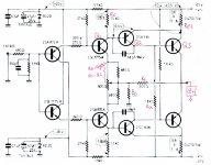
Attachments
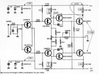

I don't see any bias adjustment. The 500ohm trim pot is more of a balance adjustment between the bias current of the top and bottom half.The bias depends from driver transistors HFE too.😀😀😀😱
seems like the 2SA872A and the 2SC1775A need to be thermal coupled on the top half to stabalize the bias drift. Also the bottom two transistors has to be thermal coupled together so the Vbe drift is cancelled out.
Last edited:
I don't see any bias adjustment. The 500ohm trim pot is more of a balance adjustment between the bias current of the top and bottom half.
seems like the 2SA872A and the 2SC1775A need to be thermal coupled on the top half to stabalize the bias drift. Also the bottom two transistors has to be thermal coupled together so the Vbe drift is cancelled out.
it will be better, but it doesn't necessarily.🙂
20W version like me a little more, than 30W.
I don't have any problems with bias drift, it increases for 20-30 minutes and then stable (bias drifting +-25 mA).
Hi
Maybe that's the reason why the author claims the output power of this amp does not double when you half the speaker impedance. This is more like the tube amp circuit.
I am going to simulate this circuit when I have time as I am too busy trying to sent out the boards. Please let me know what do you think.
Thanks
That is the strange thing from the original article. Have you done the simulation of the output stage, I didn`t have the time?
That is the strange thing from the original article. Have you done the simulation of the output stage, I didn`t have the time?
No, I am really busy trying to send my boards out tonight. I'll try to find time to do it this weekend.
But I am very intrigued with this design. It makes a lot of sense when he compare with the tube amps. Normal SS OPS are straight voltage amp with very low impedance. Efforts are made to make the output impedance as low as possible. So if the load impedance change with frequence, the power transfer to the load change with frequency also.
This design is kind of a control current source. It's the current that drive the load, so when the impedance of the load change, the voltage change along with it. So the characteristics are totally different from the conventional amp.
Granted it has GNFB, but the loop gain is low and you really don't get the full effect of the normal closed loop feedback benefit as much.
- Home
- Amplifiers
- Solid State
- Hiraga 20W class A