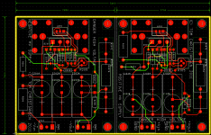
HV regulator boards are taking shape
Folks,
I figured I should let you know where I'm at with the prototyping... Stare at attached.
Note that C101, C102, C103, R107, C201, C202, C203, R207 have multiple options. The idea is to allow for either a film cap or an electrolytic cap in case of the capacitors. The resistor options allow for using 3W, 5W, or 10W types. This allows for a fair amount of flexibility as far as input and output voltages go.
R200 is in series with the input to the negative regulator. It ensures that the cascode device, Q201, doesn't fry in the event of a short circuit on the negative supply.
The image shows two boards on one panel. The end result will be two separate boards.
I plan to build a prototype using toner transfer before committing to a PCB fab run. I'll let you know how it goes.
~Tom
Attachments
Last edited:
I disagree, actually. Run a sim of the loop gain and it's pretty easy to convince yourself of the advantages of the IC regulators. You do have to ensure that the cascode device will operate within its SOA under all operating conditions. If the cascode fries, so will the IC.
It's the same level of reliability for the discrete regulator. If the pass device in the discrete regulator fries due to operation outside its SOA, the regulator won't regulate.
~Tom
Running a sim closed-loop may hide some of the real problems.
If you try it open loop you can see the effect of the two poles formed within the stack.
The first, formed by the darlington input and the large base resistor, is at 20 or so kHz.
The second is formed by the current limit resistor plus the dynamic impedance of the 317 output transistor [ a few ohms at likely currents], against the output & load capacitance.
Provided you use all the values specified by Maida AND your load is broadly resistive, the transient response is reasonable. But for instance, increasing the load capacitance causes the second pole to fall lower down the audio spectrum, so that the reaction with the first pole gives a phase response going up & down like a *****'s drawers across your load spectrum - hardly conducive to a neat transient behaviour.
This is the reason that Maida specified the output network of 2.7R and 1uF MKT [or 1R and 1u elko if you cheap out], where the ordinary 317 circuit is quite happy with big capacitor loads. In a Maida, applying the capacitive load without the resistor would probably induce oscillation, for many C values.
Anyway - my point is that for a general-purpose regulator, where you don't know the nature of the load, and you might want to add capacitors anyway - it is better to have a regulator with a fairly low open-loop impedance. Getting plenty of loop gain is no problem with some discrete transistors, as Elvee has shown.
Rod,
I see your point and do agree that open-loop sims are needed to reveal the poles and zeros of the loop. I think I misunderstood your comments about reliability which put me off for a bit. Anyway... I think your concerns are valid.
The prototype I threw together from the schematic/pcb in my post of yesterday actually works really well. It regulates fine with no load. However, it does not survive start-up into a low-impedance load. On the lab bench I use light bulbs for a load. Four 25 W, 120 V bulbs in series present 200-some ohms with cold filaments. If I bring the input voltage up slowly, the regulator works fine. But turn-on by the flip of a switch leaves me with $7 of dead silicon... Relying on the emitter/source resistor of the cascode to provide any current limiting function is not reliable. I may have to swallow my pride and use a discrete regulator... 🙂
On the upshot, this means I could get to have some fun by using a 0C3 or similar as the reference...
The need for the regulator to start up into, basically, a dead short is due to the Loftin-White circuit. The regulators "sees" a discharged 47 uF cap in series with a 600-ish ohm resistor on start-up. The regulator will need to charge the cap to about 400 V without dying. After that, the load current is 90~100 mA. SOA limit on the pass device I'm using is 300 mA at Vds = 600 V, Tcase = 25 C.
~Tom
Last edited:
How to straighten the tempco of this circuit
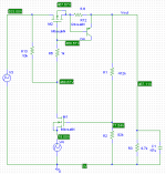
Attached shows my latest incarnation of the high voltage regulator. It's pretty straight forward. I chose MOS to avoid base currents of BJTs. Power BJTs tend to have rather crappy beta, hence draw an unfair amount of base current. This forces resistors to be lower, hence burn more power. I have a small-signal BJT handling current limiting by sensing the voltage across a 5.6 ohm resistor. The current limit is about 130 mA.
I still need to add the compensation network so this circuit is by no means complete.
However, as an engineer and, thus, perfectionist there is one thing that bugs me a little bit. Due to the Vgs variation versus temperature of the error amp MOSFET, the output voltage varies about 1 % across temperature (0 C --> 125 C). I would like to straighten that out a bit. Does any of you have ideas on how to do this?
The temperature of the error amp device and temperature compensating device need to track. So they could be two identical devices mounted back-to-back on the same heat sink. Easy. One could be hooked as a diode in series with the lower resistor (R2) in the feedback network. But in order for this to work, the two devices will need to operate at the same current density, hence, I need to burn 5~6 mA in the feedback network. A bit rich for my blood...
Any other ideas?
~Tom
Attachments
I assume R3 is your dummy load?
A 1% thermal error is not exactly the end of the world, but you can use a diode in the reference string to compensate if your circuit is really that critical. But that 1% error isn't even close to being the performance limiting factor- your main problem will be poor regulation because of the low feedback. A speedup cap across R1 will help, but not nearly as much as increasing the reference voltage to something more like 100-200V.
If it were me and I didn't want to use a Maida (big "if"- they have always performed reliably and well when I've used them), I'd have the error amp be a CCS-tailed diff amp so the the reference voltage could be filtered. I'd make the error amp with bipolars to improve regulation. You'll want to stopper the MOSFET gate- R6 is on the "wrong" side.
I assume R3 is your dummy load?
Yep.
A 1% thermal error is not exactly the end of the world, but you can use a diode in the reference string to compensate if your circuit is really that critical.
That's certainly true. 4~5 V variation on 470 V is not the end of the world by any means. I can always adjust the voltage at hot temp as the devices will dissipate a fair amount of power and run hot anyway.
But that 1% error isn't even close to being the performance limiting factor- your main problem will be poor regulation because of the low feedback. A speedup cap across R1 will help, but not nearly as much as increasing the reference voltage to something more like 100-200V.
I haven't sim'ed regulation yet. But the loop gain is on the order of 60 dB so I would be surprised if the regulation was that bad. Not thereby saying it couldn't be improved. In fact I would like to improve it.
If it were me and I didn't want to use a Maida (big "if"- they have always performed reliably and well when I've used them), I'd have the error amp be a CCS-tailed diff amp so the the reference voltage could be filtered. I'd make the error amp with bipolars to improve regulation. You'll want to stopper the MOSFET gate- R6 is on the "wrong" side.
Correct about R6. Oops... Good catch.
I tried several incarnations of the Maida regulator. The main problem is that the current limiter is relying on the Vbe/Vgs of the cascode along with the drop-out voltage of the LM317 to work. For resistive loads or small capacitive loads, this is not an issue. But in my case, I'm driving 47 uF with the regulator so the regulator will need to be able to survive starting up into a dead short. Aside from changing the topology of the amp I'm supplying (which I have decided not to do), there's really no way around it. I like the Maida as well, but for this application, I'm afraid it's out.
I'd like to filter Vref as well. Diff pair... DUH! Why didn't I think of that.... 🙂 That would also eliminate the thermal issues associated with the Vgs of the error amp in the circuit above.
I'll take another spin through the sim cycle...
Thanks for your inputs.
~Tom
One thing that helps you is that the impedance doesn't have to be ultra-low. You're running a tube circuit and it's class A.
Have you looked at Jan Didden's HV regulator? Very nice design. I've used one on my breadboard with excellent results, and it will be in my next power amp.
Have you looked at Jan Didden's HV regulator? Very nice design. I've used one on my breadboard with excellent results, and it will be in my next power amp.
Did you consider the HV Regulator from Horowitz and Hill? I modified one of my Heath HV supplies to use it.
Did you consider the HV Regulator from Horowitz and Hill? I modified one of my Heath HV supplies to use it.
The one with the op-amp as the error amp (2nd Ed, p 369, fig. 6.47)? Looks like a pretty neat circuit.
~Tom
Something pretty similar done by Joe Curcio (again, I built a dozen or so and no field failures). He published one of his in the first issue of Glass Audio- it used a Maida for a reference, then an opamp on floating rails for the error amp. The versions I built (except one) had a reference voltage derived from a FET current source pushing though a resistor, then RC filtered.
Something pretty similar done by Joe Curcio (again, I built a dozen or so and no field failures). He published one of his in the first issue of Glass Audio- it used a Maida for a reference, then an opamp on floating rails for the error amp. The versions I built (except one) had a reference voltage derived from a FET current source pushing though a resistor, then RC filtered.
I'm familiar with Curico's design. I happened to bump into him at work and he showed it to me then. It's a pretty sleek design. It's a Maida regulator with a couple of op-amps buffers. The op-amps supply voltages that are a zener drop less than the output voltage from the Maida regulator. These outputs are not current limited. The main output is theoretically current limited by the Maida regulator.
Or maybe you're talking about a different design.
I'm confident I can crack this nut. I've designed many LDO's at work but all at 3.3 V or below. Same principles apply at high voltages, though, one has to be mindful of SOA limits, power dissipated, and such. I find it rather ironic that I spend a lot of time at work ensuring that 2.5 V devices don't blow up due to over-voltage, but at home have headroom issues with my high-voltage supplies... 🙂
~Tom
your main problem will be poor regulation because of the low feedback.
SY: When you say regulation do you mean load regulation or line regulation? Or both?
~Tom
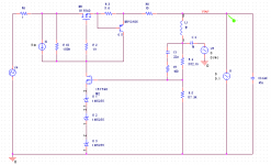
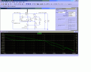
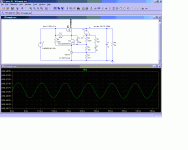
I ran a couple of sims on attached (sorry for the crappy image quality). Ignore L1, C2, V5. They are used for the open-loop analysis (in that case L = 1 kH; C = 1 kF; V5 = -1 VAC and Vout shows the loop gain).
Here are the results:
Line regulation: 75 dB up to 10 kHz (70 dB @ 30 kHz).
Output impedance: 100 mOhm (up to 30 kHz)
75 dB DC loop gain, 30 kHz UGBW, PM = 74 deg, GM = -28 dB.
That's pretty respectable. Of course, I'm not going to use IRF840's as they won't handle the voltage, but that's what I had models for. It shouldn't be too far off from reality.
There are features I could wish for that I don't see implemented in this circuit. Soft start being one. Though, the current limiter takes care of that - kind of. It would also be nice to have a filtered reference voltage. But in terms of simplicity this is tough to beat.
~Tom
Attachments
Last edited:
Looking at the zener string, this is an achilles heel...poor dynamic regulation (high impedance) will cause temp/voltage variations and is noisy. I use a string of TL431's which are the perfect sources, but what's missing in your diagram is zener voltage feed otherwise it won't start.
My experience a fast zener or TVS is required across mosfet G/S imperative against spikes. This circuit enclosed I use alot cobbled from the junk box. Notice the extra cap ripple rejection feed. That makes a BIG difference. The cue in HV power supply circuits is to avoid too much gain that can cause oscillations so ferrite beads to fitted to mosfet drain & gate.
One can improve these circuits no end but they are reliable. A similiar approach can be done for the high current 6.3V, with a very low drop out but that can come later.
richy
Attachments

This kind of topology can be implemented using a TL431 as a "supertransistor", having superior gain and voltage stability.
Here is an example, cascoded with a MOS for high voltage operation.
The circuit just illustrates the concept and lacks protections: zeners across G-S of MOS transistors, current limiter etc.
The transistor types also are unsuitable, M2 in particular, they were picked for a quick sim, but it shows the principles.
The circuit has decent performances and good stability for a minimal complexity.
Attachments
Last edited:
Tom, you want C1 from your schematic (the speedup cap) to be a lot smaller. 1 or 2uF is enough to get you the benefit of low source impedance at audio frequencies without excessive slowing down the regulator recovery from load changes.
Rich's point about the Zener noise is spot on. That's one reason that using a diff amp for the error amp is useful- you can filter the noise more easily since the base or gate of a transistor is a higher impedance point than the emitter or source.
Rich's point about the Zener noise is spot on. That's one reason that using a diff amp for the error amp is useful- you can filter the noise more easily since the base or gate of a transistor is a higher impedance point than the emitter or source.
Tom, you want C1 from your schematic (the speedup cap) to be a lot smaller. 1 or 2uF is enough to get you the benefit of low source impedance at audio frequencies without excessive slowing down the regulator recovery from load changes.
Yeah, I wasn't too thrilled with the 22 uF either. It does give me higher phase margin, though. But I need to find a better compensation scheme.
Rich's point about the Zener noise is spot on. That's one reason that using a diff amp for the error amp is useful- you can filter the noise more easily since the base or gate of a transistor is a higher impedance point than the emitter or source.
I get that.
I'll actually be using a 0A3 in the final circuit. Not a zener. I just threw in the zeners in the simulation as the models were readily available. I understand that zeners are noisy. The question is if the noise on the output of the supply will be audible in the speakers on the amp it's driving. Unless the reference is the dominant noise source, there's really no reason to address its noise.
I did actually try to design a diff-amp based regulator. I was able to get good results in the simulator, but it uses a lot more devices than the simple regulator. More importantly, it relies on the use of PNP/PMOS devices. Sourcing PNP/PMOS devices that can tolerate 600+ volts Vce/Vds is not easy these days. Neither Newark nor Digikey carry them.
~Tom
I'd kill for some 1kV PNP/PMOS.
I did build a +/- 500V Maida-type supply and used 500V PMOS/LM337 for the negative side. I put a 400V Zener across the PFETs it and the supply is reliable. Raw supply is 560V.
I did build a +/- 500V Maida-type supply and used 500V PMOS/LM337 for the negative side. I put a 400V Zener across the PFETs it and the supply is reliable. Raw supply is 560V.
I'd kill for some 1kV PNP/PMOS.
I did build a +/- 500V Maida-type supply and used 500V PMOS/LM337 for the negative side. I put a 400V Zener across the PFETs it and the supply is reliable. Raw supply is 560V.
I've done the same thing. I found a bipolar darlington power transistor and an LM337. Worked great. However, for my positive regulator I cannot use a Maida regulator (have tried several incarnations of it) as its current limiter is not reliable enough. My load is an Loftin-White amp that presents 47 uF in series with 600 ohm to the supply. In other words, a dead short on start-up. The Maida does not survive that. Not using a 3 A bipolar nor a 16 A MOS. It's a rather effective way of turning silicon into slag... 🙂
Hence, I'm designing my own regulator.
~Tom
- Status
- Not open for further replies.
- Home
- Amplifiers
- Power Supplies
- High Voltage Regulators (Maida or zener)