PM of 29 - well below 45 which I consider 'minimum', is not acceptable.
How is it without snubbers?
Attachments

I used my schematic/sim, and l modified it it to match yours.
Same results. PM 27.
Weird - I tried my own latest schematic/sim without any changes, and PM also comes at 28.
If I change feeback cap C8 from 220pF to 120pF (as it was in the original post #1), PM goes back to 60.
At some point this cap was even at 82pF... (post #71).
I guess this cap has been adjusted in the real build to correct square wave response..
Will need to check my posts from the testing stage...
Yes: post #107 documents change from 82pF to 220pF.
So I guess that's the difference between sim and real life.
Start with 82pF, and check the squares on the oscilloscope. Perhaps for your build square waves will be fine.
If you have overshots like me, try increasing C8.
Last edited:
I think increase the lead compensation capacitor value from 82pF to 220pF destroys the stability margins significantly .
Last edited:
Well, hard to say who is right: sim or real build.
Obviously they are not in sync.
However in real life amp is solid and stable, so I guess my vote goes for reality, not for the sim..
This kind of things are, I'm afraid, expected.
Obviously they are not in sync.
However in real life amp is solid and stable, so I guess my vote goes for reality, not for the sim..
This kind of things are, I'm afraid, expected.
>Do you use an LR network at output?
Yes. Always.
I don't put it on the amp's PCB because I have it on the speaker protection board that I use for all amps.
Yes. Always.
I don't put it on the amp's PCB because I have it on the speaker protection board that I use for all amps.

>Which schematic you're referring to?
I guess this idea can be applied to any complementary mosfet OS, E.g. in the last amp built in this thread. I think I'll try it.
And of course crowbar DC protection can be added to any amp.
I guess this idea can be applied to any complementary mosfet OS, E.g. in the last amp built in this thread. I think I'll try it.
And of course crowbar DC protection can be added to any amp.
NMOS,
In my quick sim this doesn't seem better than 'normal' quasi.
Are you sure collector of T12 should be grounded? It's impossible to bias OS correctly like this. Problem disappears if T12 collector goes to the OUT instead of GND.
There is also crossover distortion present...
Can you share your sim?
In my quick sim this doesn't seem better than 'normal' quasi.
Are you sure collector of T12 should be grounded? It's impossible to bias OS correctly like this. Problem disappears if T12 collector goes to the OUT instead of GND.
There is also crossover distortion present...
Can you share your sim?
I prefer Hexfet N Channel Mosfets in the output stage, there is no advantage to using P Mosfets, only disadvantages
I changed the schematic and add DC protection.
I'm in the process of designing PCB board with the changes
Manufacturers like Denon have used just N-types in their output stages for some of their designs and they work fine. I am interested in how this develops.

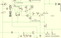
I have tidied up the Sprint Layout design and made the following changes:
1. Converted the OPAMP power supply Zener resistors to vertical mounted types so that if 2-3W resistors are preferred for heat dissipation, then they will fit. The 1W resistors were able to be fitted horizontally Ok with only minor spacing changes, but this option is more flexible.
2. Used larger footprints for the box caps (2.2u) since they are a bit wider than the 100n versions.
3. Used 10mm resistor pad spacing for most of the resistors to avoid issues with leads.
4. Used larger footprints for the Fet resistors with 4.5mm width and 15mm pitch so metal oxide resistors will now fit Ok.
5. Used correct footprints for the 5mm LEDs so they should fit much better.
6. Corrected the slight errors in the TO220 pad spacing and tweaked the spacing of those devices to accomodate resistors between the heatsinks.
7. Corrected the minor spacing difference of the Fets. - now all the same
8. Removed vertical fuses but these can be added for those who like fuses on amp boards. There is enough space to do that as the fuse holders are 12mm dia with 8mm pitch, if the supply caps are reduced to the original footprint size.
9. Increased footprint size of the 220u filter caps to 12.5mm
10. Moved the 220u inverting input cap so that its base mounts flat on the PCB.
11. Changed the gate protection diodes to vertically mounted.
12. Replaced the "Fet" footprints with Fet footprints - original had BJT transistor footprints.
13. Changed footprint of caps for OPAMP power filtering so they are electrolytic (6.5mm) and will now fit flush to PCB.
There remains the original discrepancies between the schematic and original Sprint Layout board with an electrolytic not "box" footprint cap used for C12 and no 22R resistors on the bases of two transistors. - What value electrolytic is actually used?
I have added as an option, C21 which is in the schematic but not on the original PCB. This cap bypasses the 1k on the Fet gates.
😴😴
Attachments
1. In my original build resistors that are placed between heatsinks for to-126 transistors, were soldered UNDER the board, so heatsinks could be closer to each other
2. I think the 2.2uF speed-up cap (C21) should be replaced with 220nF.
2.2uF is too much for fet OS (2.2uF would be more appropriate for BJTs, but for fets 220nF will be enough). In my build I used 1uF.
I see two of them on the PCB???
3. I was trying to avoid placing tall components in front of the output fets, to avoid obstruction of the screw/bolt, in case when transistor has to be unscrewed from the hetasink. Even as it is, I had to used special tiny wrench for hex bolts to screw fets to the heatsink. Could not fit normal screwdriver to do this...
4. C12 cap it could be anything from 1uF to 10uF. I used 10uF electrolytic.
5. C16 cap (47nF) can be anything from 22nF to 100nF (ceramic is ok). I used 39nF in my build.
My latest sim file attached.
C8 feedback cap was originally 82pF (perfect value according to the sim), but in real build was corrected to 220pF to fix square waves response.
Attachments
Last edited:
May I ask how you decide on the NMOS PMOS combination ?
Only to match ciss, or Yfs, or ??
I have seen in this thread :
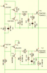
FQA36P15 2550pF
FQA27N25 1500pF
FQA40N25 3100pF
FQA46N15 2500pF
So one PMOS only but 3 different NMOS.
I wonder how they affect the results.
Thanks,
Patrick
Only to match ciss, or Yfs, or ??
I have seen in this thread :
FQA36P15 2550pF
FQA27N25 1500pF
FQA40N25 3100pF
FQA46N15 2500pF
So one PMOS only but 3 different NMOS.
I wonder how they affect the results.
Thanks,
Patrick
Different Ciss values should not be a problem if you use different gate stoppers for N and P fets.
As long as RC is const, it should be fine.
Same thing happens with lateral mosfets, even supposedly complementary pairs have different Ciss..
FQA40N25 and FQA36P15 is a commonly used combo, since FQA36P15 doesn't have a perfect complementary sibling. Many amps built with them. If I remember correctly, this combo was recommended by Aksa long time ago...
I used FQA40N25 and FQA27N25 paired with FQA36P15 in 2 amps, and they both seem to sim and work perfectly.
I'm sure IRF240/9240 also could be used.
Last edited:
- Home
- Amplifiers
- Solid State
- HexFet Amp Based on Philips AH578 and LMK