MJL21193 said:In general, do you believe it is good as is for my needs? Every thing looks good on the simulation - THD, wave shape, voltages and current.
Have I done enough tinkering?
Hi MJL21193,
I'm not really qualified to give you a judgment on your design, especially with 56v rails.
I'm a perpetual tinkerer, so I get very little done. There a lot to be said for those that jump in a get it done.
regards
Greg Erskine said:
There a lot to be said for those that jump in a get it done.
I'm a tinkerer, but not an endless one. I have to get it done (eventually).
Wow! I just took the time to model DX's amp and it's one for the books. THD over 3% at 1KHz. I think I'll pass...
MJL21193 said:Wow! I just took the time to model DX's amp and it's one for the books. THD over 3% at 1KHz. I think I'll pass...
Sorry going OT, but Carlos designs his amps using a simulator as well and I'm sure he wouldn't be happy with > 3% THD either. So I wonder what's happening?
regards
Greg Erskine said:
. So I wonder what's happening?
It is the first version that I modeled. Oops. The second one looks better, but I haven't modeled it yet.
Sorry for the mix-up.
MJL21193 said:Hi Lazy Cat,
I'm not sure hat you are referring to. Look at this latest schematic and comment in relation to the components on it. For example: put a 5K resistor between Q56 and Q78.
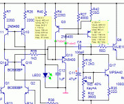
Updated schematic. How many now? Not much similarity between this one and the first one, except the output stage.
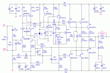
OK, let me suggest a better way of doing the transistor clamp. The diff pair is current limited by the emitter current source or resistor. So, it is best to clamp the base drive to the beta multiplier, we want the transistor off and a high impedance until it turns on during overload. The collector is a high impedance so you want a PNP transistor with the emitter connected to the positive rail through a resistor to allow adjustment of the current limit point. The base goes to the base of the VAS to sense the Vbe drop. Here's a picture where I tested it in the 990, I lowered the VAS emitter resistor to 20 ohms which I think is probably a good value for your design. R24 in the collector provides a bit more protection:
http://baselaudiolabs.googlepages.com/990_clamp.PNG
So, I've been meaning to suggest some emitter degeneration in the VAS, keep it small so that you do not loose positive swing there.
Base stoppers on the output devices might help stop local oscillation there.
I like the idea of 10 ohms to isolate the front end supply rails from the drivers/outputs.
I see you upped the diff pair degeneration to 220 ohms, I think this is a good idea, helps keep the front end linear, but you'll want to check distortion performance as you add degeneration which will lower your open loop gain.
You really should have a look at the loop gain and phase margin and perhaps make some adjustments for stability. Look at low frequency to see if your bootstrap cap is large enough.
I'm always looking to eliminate electrolytic caps, don't know why Self called out a 47uF across the Vbe multiplier, 1 uF or even .47 film should be fine.
I've been meaning to say that you might run the VAS at 10 mA, then looked up the part and see that it is an 8A 50W part, where it's beta begins to be spec'd at 100 mA. You could up this to 20 or even 50 mA which would be unusual for an amp like this but might work out better given how large those devices are. You'll want a good heat sink on that part at these higher currents. I would not go higher than 50 mA due to SOA considerations and the high supply voltage that you're using.
Pete B.
PB2 said:
OK, let me suggest a better way of doing the transistor clamp.
Yes this is more effective. It eats some power (down 4watts to 147W into 8 ohms), but it solves both the >20KHz clipping and keeps the current through these devices down.
I adjusted the resistor values to give the best distortion, while keeping an eye on the VAS current.
Thanks Pete. 🙂
Here's what I did:
Attachments
A simpler way is to replace Q3 with a series string of four 1N4148's to clamp the negative swing at the base of Q13.
Cheers,
Glen
Cheers,
Glen
PB2 said:
I've been meaning to say that you might run the VAS at 10 mA, then looked up the part and see that it is an 8A 50W part, where it's beta begins to be spec'd at 100 mA. You could up this to 20 or even 50 mA which would be unusual for an amp like this but might work out better given how large those devices are. You'll want a good heat sink on that part at these higher currents. I would not go higher than 50 mA due to SOA considerations and the high supply voltage that you're using.
I took your suggestion, increasing VAS current to >12mA. This allowed me to reduce the emitter resistors in the differential pair, thereby reducing distortion even further (presently it's at .036% THD at 20KHz at full output).
What are the advantages of running the VAS with high current?
The changes I've made:
Attachments
MJL21193 said:
I took your suggestion, increasing VAS current to >12mA. This allowed me to reduce the emitter resistors in the differential pair, thereby reducing distortion even further (presently it's at .036% THD at 20KHz at full output).
What are the advantages of running the VAS with high current?
The changes I've made:
It's a large device, the internal capacitances are larger, it needs more current to get into it's best operating range. If you look at the spec sheet you can see that Ft, Hfe etc. drop off at reduced current. I would not worry too much about it, but it might be interesting to try 20 to 40 mA. While it might be tempting to run it up to 100 or 200 mA where the parameters look better, there's too much voltage on the VAS to do that safely.
I also noticed that your VAS is not a very high beta device which means that it is completely reasonable to leave out or reduce even further the VAS emitter resistor. I didn't notice the low beta previously when I said to add that resistor.
I'm surprised that you get enough sense voltage where you have the base of the clamp connected. I'd connect it to the base of the VAS, not sure what's going on in your design. Might help if you show the full schematic.
Pete B.
PB2 said:Please drive it into overload and check waveforms and device currents. I see over 50 mA in the beta multiplier, your Q13 when I remove the Baker clamp in the 990, way too much. Some form of current limiting is usually needed when a Beta Multiplier is used.
Pete B.
Noticed that Self does not use any current limiting on his beta multiplier. I've not read his pages carefully but I hope this is not an oversight in his designs. He does not use emitter degeneration on the VAS which makes the situation even worse. I'd expect that transistor to fail under clipping in his design.
Pete B.
PB2 said:
I'm surprised that you get enough sense voltage where you have the base of the clamp connected. I'd connect it to the base of the VAS, not sure what's going on in your design. Might help if you show the full schematic.
Here's the latest schematic update. I have changed some values and moved the clamp base. There is a definite trade-off with this clamp - higher distortion. I did my best to compromise.
VAS current is now ~15mA. I tried higher but the distortion level went wild, and >20 KHz clipping shows a big jump in current flow.
Quiescent current is sitting at 88mA (best distortion at this setting).
I have added the 10 ohm R's on the rails to isolate input stage from output and I will ad base stoppers to the output devices.
Look it over and let's see if we are getting close to a decent amp.
Attachments
MJL21193 said:
Here's the latest schematic update. I have changed some values and moved the clamp base. There is a definite trade-off with this clamp - higher distortion. I did my best to compromise.
VAS current is now ~15mA. I tried higher but the distortion level went wild, and >20 KHz clipping shows a big jump in current flow.
At risk of starting WWIII;
This is completely wrong and it simply not work in the real world. The operation of your VAS over-current clamp is entirely dependant on Vbe of both the VAS and clamping transistor.
This is why the THD goes through the roof when the VAS current is increased - Vbe of the VAS transistor rises and the clamping transistor is biased on, even when the amp is just idling.
The clamping transistor must NOT be biased on during normal operartion otherwise it will introduce distortion. The purpose of the clamping transistor limit the VAS current ONLY during clipping.
The way you had it connected the first time is the correct way - with the base of the clamping transistor connected to a emitter degeneration resistor for the VAS transistor.
Your emitter degeneration resistor was 20 ohms, giving a VAS current limit of approximately 30mA. The VAS clamping transistor will begin to turn on with about 0.6V at it's base - which happens when 30mA flows through the 20 ohm resistor.
Cheers,
Glen
I actually agree to some extent. The very large emitter resistor is making your clamp operate in a highly linear way, when you want it highly non-linear. Any sense point will do, you could split the 100 ohm load and go closer to the rail. Or you could go back to the 20 ohm and sense at the emitter, I was thinking of the JE990 where 30 mA would be too much. You've got an 8A VAS transistor - LOL. If you up the VAS bias to 15 mA you'll want the clamp up around 40 to 50 mA so that it can swing to the rail.
You could try the diode string but you don't get a lot of adjustment with it.
Also your VAS R load of 4K+4K with a 56 V supply yields 7mA not 15.
I think that you're close, it's a lot of work, but we've identified a problem with beta multipliers and it's going to take a bit of time to find a good solution.
Notice how jcx does the emitter follower Q11 here:
http://www.diyaudio.com/forums/attachment.php?s=&postid=209401&stamp=1058764592
That configuration might solve all your problems because Q11 in his diagram, only sees the Vbe drop of the VAS. It is protected in a voltage sense and you could use the much higher beta BC550 because there is so little Vcb voltage. Obviously, you might have to make some other adjustments but it should work. I've never tried that configuration but I plan to soon.
I'm planning to do a power amp derived from the 990, similar to yours, so I'm interested in the results of your simulations.
Pete B.
Q13 is turning on during normal signals.MJL21193 said:
Here's the latest schematic update. I have changed some values and moved the clamp base. There is a definite trade-off with this clamp - higher distortion. I did my best to compromise.
VAS current is now ~15mA. I tried higher but the distortion level went wild, and >20 KHz clipping shows a big jump in current flow.
Quiescent current is sitting at 88mA (best distortion at this setting).
I have added the 10 ohm R's on the rails to isolate input stage from output and I will ad base stoppers to the output devices.
Look it over and let's see if we are getting close to a decent amp.
I contend that protection must never trigger on valid input signals.
the Vbe of Q13 starts to turn on at around 400mV. You must select it's monitoring voltage so that it never sees a signal of around 400mV when you drive the amplifier to maximum power.
Split that 100r resistor and monitor the current in the top half of the split resistor. If I were doing this for a normal VAS without the EF (beta enhancer) set the monitoring resistor to allow 3times the VAS quiescent current to generate 600mV of Vbe in the protection transistor. Use the sim to identify the currents flowing in this section and calculate what value of monitoring resistor is required to ensure Q13 does not turn on at maximum power.
If you don't do that it will be audible.
I don't think so.G.Kleinschmidt said:
Your emitter degeneration resistor was 20 ohms, giving a VAS current limit of approximately 30mA. The VAS clamping transistor will begin to turn on with about 0.6V at it's base - which happens when 30mA flows through the 20 ohm resistor.
As stated in my previous post most transistors start to turn on at around 400mV not 600mV.
They are in their normal operating range when Vbe ~=600mV.
MJL21193 said:
Here's the latest schematic update. I have changed some values and moved the clamp base. There is a definite trade-off with this clamp - higher distortion. I did my best to compromise.
VAS current is now ~15mA. I tried higher but the distortion level went wild, and >20 KHz clipping shows a big jump in current flow.
Quiescent current is sitting at 88mA (best distortion at this setting).
I have added the 10 ohm R's on the rails to isolate input stage from output and I will ad base stoppers to the output devices.
Look it over and let's see if we are getting close to a decent amp.
OK, I did a more complete simulation of a very similar power amp, more based on the 990, but very similar to what you have. I was also unable to get the best performance with the transistor clamp, so we should step back and take another look at the problem. The simulator was giving some very strange results with the clamp that did not pass a sanity check in any way what so ever. I don't usually see this with LT Spice. I did not try altering any of the simulation controls to fix this, because I just don't have the time.
Back to the current limit issue. The other front end transistors do not have a problem because they either have a resistor or current source limiting Ic. The simple solution, and it works fine in my simulation is to put a 5.1K resistor in the collector lead of your Q13. With normal signals only a very small signal is produced at the collector. However under clipping conditions the current is limited to about 10 mA, (300 mA without the resistor) the key is that there is a large drop on the resistor under this condition and so Q13 does not see the combination of high voltage and current as it does without the resistor. It is an excellent solution.
I get .002 ish THD at 20 kHz just below clipping into 8 ohms, and .001 ish at about 46 Vp out.
Pete B.
G.Kleinschmidt said:
At risk of starting WWIII;
No problem Glen,
I have a few fields of knowledge where I consider myself well versed; basic electronics is not one of them. I'm learning though, with the help and incentive I'm getting here.
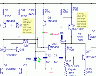
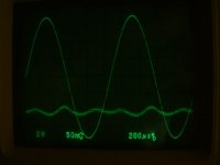
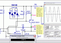
When you initially suggested it, I tried the string of 4 diodes to replace the clamping transistor. It worked effectively but it had the current going through Q4 too high and as seen in the graphic, distortion was big and the waveform is visibly distorted.
Any ideas on fixing this?
Also, I'm learning that I can't trust the distortion readings or the oscilloscope when these measurement "probes" are in the circuit. Somehow, they corrupt the output.
Attachments
PB2 said:
I was also unable to get the best performance with the transistor clamp, so we should step back and take another look at the problem.
The simple solution, and it works fine in my simulation is to put a 5.1K resistor in the collector lead of your Q13.
Hi Pete,
Maybe this is the reason why there isn't a clamping arrangement in D. Self's Blameless. Can my selection of components take occasional clipping on transients? Not that I will ever let it go that high, but hey, I don't live alone.
This limiting resistor idea sounds like the ticket. I will try it out.
MJL21193 said:
No problem Glen,
I have a few fields of knowledge where I consider myself well versed; basic electronics is not one of them. I'm learning though, with the help and incentive I'm getting here.
When you initially suggested it, I tried the string of 4 diodes to replace the clamping transistor. It worked effectively but it had the current going through Q4 too high and as seen in the graphic, distortion was big and the waveform is visibly distorted.
Any ideas on fixing this?
OK, unfortunately that wouldn't have worked at all because the diodes need to be the other way round. Also, the diode clamp must be used in conjunction with emitter degeneration of the VAS transistor, otherwise it wont work either.
Connect the diodes the other way round (anode to the positive rail), get rid of R4 and put an emitter degeneration resistor on Q4's emitter.
Start with, say, 30R. By adjusting this value, you can set the current at which the VAS is clamped.
Cheers,
Glen
- Status
- Not open for further replies.
- Home
- Amplifiers
- Solid State
- Help with this amp? A patchwork product of simulation