PB2 said:I'd add a Baker clamp as seen in the 990...Check to see what your design does when driven 20 - 50% into overload at 20 KHz. Like it or not you will probably hit some clipping from time to time.
With just .3Vpp it turned nasty. Took a while to educate myself a little on what a Baker clamp is, but I think I've got it.
Look at the attached pic. I don't know if this is exactly it, but it seems to work, doubling the clipping limit.
Attachments
MJL21193 said:
With just .3Vpp it turned nasty. Took a while to educate myself a little on what a Baker clamp is, but I think I've got it.
Look at the attached pic. I don't know if this is exactly it, but it seems to work, doubling the clipping limit.
Sorry, I should have mentioned that it goes on the VAS, no not on the diff pair. Take a look at the JE-990 schematic, see page 3 here CR4 is the Baker clamp:
http://www.johnhardyco.com/pdf/990-2007.pdf
.3V? I would have expected 3V in for a typical amp. What you should hope to see is clean clipping.
Pete B.
G.Kleinschmidt said:
I’d omit C19 and R28, connecting C12 directly across the LED.
You are using a bit of a big transistor for Q14, which has high collector-base capacitance. With the high voltage signal swing at it’s collector, modulation of the bias voltage (and LTP tail current) via Cob at high frequencies could be an issue.
A nice, low ESR capacitor for C12 would in order. Maybe even another one from the base of Q3 to the negative rail. At 22k R9 is a bit large too. Drop to around 1k or so.
Hi Glen,
The circuit you decided to pick on and take the hatchet to was a days work to get right!😱
First, C19 is innocent, not hurting anyone. Second, the rest of this circuit has a magical ability to tame startup transients. Changing any value here and the trouble begins.
No, I don't have a clue how this is, but it works.
Originally Q14 was 2N5550, but it would run too hot (too much current?). I then tried boot strap but abandoned it and went with a tougher transistor (boot strap is a true POS).
How is the high capacitance a problem? Stress the input stage? Would it be better to cascode a couple of BD139?
Remember, I'm working with what I've got.
PB2 said:Did you intend to run this as a Class A amp?
You've got nearly 1 Amp through each output device. You need to reduce this to around 100 mA to have reasonable idle dissipation. Recheck your distortion, it will probably be higher.
Hi Pete,
The measurements shown are with the amp running at full output at 1KHz into 8 ohm load. Still had too much forward current(324mA idle). Reducing R18 pot to 40% gets this down to ~100mA.
PB2 said:
Sorry, I should have mentioned that it goes on the VAS, no not on the diff pair.
.3V? I would have expected 3V in for a typical amp. What you should hope to see is clean clipping.
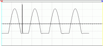
I have input sensitivity at 1.2Vrms (3.380Vpp) for this amp. Above that, clipping starts. So at 3.780Vpp, there was complete wave deformation (at 20KHz). This doesn't happen at lower frequencies.
Now that I look at the schematic that you pointed to, I see that it was suggested in an earlier post. X-pro, in post #5 recommended it. I tried it with the device he mentioned, but it caused the output to go to rail voltage.
Now I have tried it with 1N4148 and have the bottom of the wave clipped and get some brutal spikes happening.
Is there a more suitable diode or is this indicative of a bigger problem somewhere else?
Here an image of what the clamp is doing:
Attachments
If you want to learn about a few more tricks for reducing distortion read about jcx's bootstrapped front end here.
I'm surprised that there's not more discussion about it:
http://www.diyaudio.com/forums/showthread.php?postid=209401#post209401
Pete B.
I'm surprised that there's not more discussion about it:
http://www.diyaudio.com/forums/showthread.php?postid=209401#post209401
Pete B.
MJL21193 said:
Hi Glen,
The circuit you decided to pick on and take the hatchet to was a days work to get right!😱
First, C19 is innocent, not hurting anyone. Second, the rest of this circuit has a magical ability to tame startup transients. Changing any value here and the trouble begins.
No, I don't have a clue how this is, but it works.
I wasn't taking a hatchet to your circuit; I was only pointing out a few little obvious things that do not look right. Apologies if I am boring you. C19 doesn’t serve a useful purpose, so there is no reason for including it. C12 does not serve any useful purpose either, connected in series with R28.
I don’t know what kind of “start up transient’s” you are referring to, or why they should be an issue. Perhaps just a quirk of the simulator?
MJL21193 said:Originally Q14 was 2N5550, but it would run too hot (too much current?). I then tried boot strap but abandoned it and went with a tougher transistor (boot strap is a true POS).
How is the high capacitance a problem? Stress the input stage? Would it be better to cascode a couple of BD139?
Remember, I'm working with what I've got.
Yes, I am aware that you are working with the parts you have. That is why I did not insist that you change them, but instead pointed out some of the potential problems of using them.
When you bias both the LTP and VAS current sources from a common voltage reference (LED1 in your circuit), some degree of decoupling is mandatory in a low distortion design to avoid signal feedback via Cob of the VAS current source transistor modulating the reference voltage and thus the LTP tail current. This can significantly degrade the amplifiers THD performance and D.Self has written about this in his book at some length, IIRC.
As it stands, you circuit doesn’t have any effective decoupling of the reference voltage, which is especially bad in this instance due to the massively over-specified (8 Ampere, 50Watt) transistors you are using for the VAS and it’s current source.
The effect may not show up in simulation either – it would depend on how well the LED model recreates the dynamic impedance of the device, for one thing.
Cheers,
Glen
G.Kleinschmidt said:
I wasn't taking a hatchet to your circuit; I was only pointing out a few little obvious things that do not look right. Apologies if I am boring you. C19 doesn’t serve a useful purpose, so there is no reason for including it. C12 does not serve any useful purpose either, connected in series with R28.
I don’t know what kind of “start up transient’s” you are referring to, or why they should be an issue. Perhaps just a quirk of the simulator?
Hi Glen,
By some stroke of luck I got the junk pile in the corner to work. It could probably be done more eloquently, I'm sure. It works though, and that's enough for me. I did try it without C12 and you are right, It doesn't do anything.
I will delete C19 - it's a leftover from the schematic this grew out of.
The transients I'm referring to are spikes and malformed waves on startup. They are supposed to be caused by the low gain of the LTP devices (what I heard). I know this is just a simulator and it might have quirks but it stopped happening when I got that divider(?) in the corner right.
I value your contribution here. I'll end up with a toaster instead of an amp if I didn't get quality advice.
You made mention of replacing Q14 with an LED. How is that configured? You also didn't say whether a cascode of two lesser devices would be a good idea.
MJL21193 said:You made mention of replacing Q14 with an LED. How is that configured? You also didn't say whether a cascode of two lesser devices would be a good idea.
Sorry, I wansn't very clear. I meant a seperate LED to bias Q14. That would totally eliminate the potential for any cross coupling between the two current sources.
A cascode would work very well, especially so since the lower transistor would only have to be a rather low power device. The only detriment would be a slightly reduced output voltage swing in the negative direction (a few volts or so).
Out of curiosity, I just did a LED test on the bench. I simply connected a red LED to my bench PSU via a limiting resistor, biased and glowing with 10mA (cathode connected to ground)
I then coupled my signal generator output in parallel with the LED via a series 33pF capacitor. With only 15V (the siggens maximum output) peak sinewave from the siggen at 20kHz, I'm getting about 5mV RMS AC across the LED.
Cheers,
Glen
Now we have a discussion on basic circuit operation and how to tune it.
More contributors, please.
More contributors, please.
MJL21193 said:
I then tried boot strap but abandoned it and went with a tougher transistor (boot strap is a true POS).
Well, I eat my words, because I'm back to boot strap for the VAS. Working with different values, I found it to be working now as good as the current source.
I have abandoned the idea of a clamping diode in the EF. In real life, I'm sure with the correct device, the results would be worth it. This amp (if running as predicted) would have to be driven pretty hard to start clipping (excess of 150Watts into 8 ohms). I know, why take the chance?
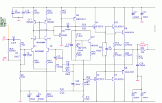
Update of the schematic where I have made a few changes. Most notable is the switch to boot strap. Also, I've changed the Vbe transistor to MPSA42 (gives better distortion?). Changed Q13 to 2N5400 as this will not see a lot of current.
A few other things here and there.
Attachments

IMHO you'll need to install some filtering in the rail after drivers because of decreased PSRR caused by the bootstrapping.
R29 looks too high for me, I would start with 1k. Or you could eliminate that resistor.
I'd ask the same.
R29 looks too high for me, I would start with 1k. Or you could eliminate that resistor.
what does r28 do?
I'd ask the same.
MJL21193 said:
Distortion goes up to .003%, so no, not as high as SymaSym. No, still a slight overshoot on the squarewave at 1K.
You should do THD-Test at 10khz, not 1khz...
Mike
AndrewT said:what does r28 do?
Dzsoni said:
R29 looks too high for me, I would start with 1k. Or you could eliminate that resistor.
Apparently in the present configuration, R28 does nothing. I've removed it altogether. I have also reduced R29 to 1.2K.
Thanks for pointing that out.
Dzsoni, more filtering in addition to C14-C17? How about I increase the electrolytics to 470uF?
MikeB said:
You should do THD-Test at 10khz, not 1khz...
Hi Mike, thanks for looking in here. 🙂
I have been doing THD test across the entire frequency range, using 1K as the mean.
I have often mention your SymAsym here as it is (so far) the best design that I've modeled.
I am re-building the SymAsym model (as I changed many values to attempt to make it operate at the higher rails) to sim again.
A head to head against the Frankenstein I've slung together here, to see if I'm on the right track..
The R29 resistor is pretty much redundant in this circuit. The idea though, is probably from an amp where the LED voltage reference is also used as the reference for the VAS current sink.
In this case, a small resistor is used in the base of the transistor serving the VAS current sink, so that if the amp is driven into clipping, the sink does not pull all of the current from the reference trying to maintain the VAS current, which in turn screws up the LTP causing allsorts of nasty problems.
For an example of that, that I can think of off the top of my head, see Marcus Gunnarsson's M250 amp.
jaycee said:The R29 resistor is pretty much redundant in this circuit. The idea though, is probably from an amp where the LED voltage reference is also used as the reference for the VAS current sink.
In this case, a small resistor is used in the base of the transistor serving the VAS current sink, so that if the amp is driven into clipping, the sink does not pull all of the current from the reference trying to maintain the VAS current, which in turn screws up the LTP causing allsorts of nasty problems.
Hi jaycee,
What you describe above is exactly the case. This part of the circuit carried over from the current source (sink?), where it was essential for smooth operation. It didn't hurt the boot strap version, so I left it in.
I will, however, delete useless components where needed.
What simulator are you using?
You might want to cascode your diff amp, if your goal is ultra low distortion. Many do this by holding the collector voltage constant. A better goal, to minimize the early effect, and to obtain lower distortion is to maintain a constant collector to base voltage. jcx does it in a very simple way here:
http://www.diyaudio.com/forums/showthread.php?postid=209401#post209401
Another way is to use an emitter follower off the emitters of the diff pair, the emitters follow the base, more or less.
Pete B.
PB2 said:What simulator are you using?
Multisim 10.
You linked to the jcx schematic earlier and I tried it out, with an input cascode using higher gain (lower voltage) BC550. Results were very good, low distortion (not as low as the other) and better high frequency clipping behavior.
I will do some more work on it but here it is. See if I did anything wrong or configured the cascode correctly.
Comments, suggestions always welcome.
Attachments
No, that's not it, I think you misinterpreted me.
Isolate the bases of Q14 and Q15 and then duplicate jcx's D1, R19, and R20. where you would use 1K for R19 and 30K for R20, the diode can be a 5V LED or a zener to drop 5 to 10 V or even 20V since your supply is so high.
On the other hand, you might want to establish the reference up from ground since the supply voltage is so high, and of course still duplicate your feedback voltage divider ratio. Let me see if I have a schematic handy to show you.
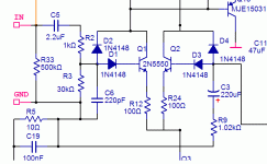
Here's the resistive divider method that I just tested out in the JE-990 with a referenced to ground. That 5V LED requires too much current to turn it fully on, just find a decent reference. The reference voltage is not critical at all:
http://baselaudiolabs.googlepages.com/res_boot_cas.PNG
Pete B.
Isolate the bases of Q14 and Q15 and then duplicate jcx's D1, R19, and R20. where you would use 1K for R19 and 30K for R20, the diode can be a 5V LED or a zener to drop 5 to 10 V or even 20V since your supply is so high.
On the other hand, you might want to establish the reference up from ground since the supply voltage is so high, and of course still duplicate your feedback voltage divider ratio. Let me see if I have a schematic handy to show you.
Here's the resistive divider method that I just tested out in the JE-990 with a referenced to ground. That 5V LED requires too much current to turn it fully on, just find a decent reference. The reference voltage is not critical at all:
http://baselaudiolabs.googlepages.com/res_boot_cas.PNG
Pete B.
- Status
- Not open for further replies.
- Home
- Amplifiers
- Solid State
- Help with this amp? A patchwork product of simulation