Does your Multisim have good BD139/140 models?
Also looking for good MJE182/172 models.
You running the student or full version?
Pete B.
Also looking for good MJE182/172 models.
You running the student or full version?
Pete B.
Here's the emitter follower method, I got very low distortion but not as low as with the resistor method, have not figured out why yet. I plan to find a better voltage reference and hopefully get rid of the cap. That's a 6.2 V zener in there, it is not critical:
http://baselaudiolabs.googlepages.com/cas_efollower.PNG
I'm using those old transistors just to stay with the same vintage as the original design.
Pete B.
http://baselaudiolabs.googlepages.com/cas_efollower.PNG
I'm using those old transistors just to stay with the same vintage as the original design.
Pete B.
PB2 said:
Isolate the bases of Q14 and Q15 and then duplicate jcx's D1, R19, and R20. where you would use 1K for R19 and 30K for R20, the diode can be a 5V LED or a zener to drop 5 to 10 V or even 20V since your supply is so high.
On the other hand, you might want to establish the reference up from ground since the supply voltage is so high, and of course still duplicate your feedback voltage divider ratio. Let me see if I have a schematic handy to show you.
Here's the resistive divider method that I just tested out in the JE-990 with a referenced to ground. That 5V LED requires too much current to turn it fully on, just find a decent reference. The reference voltage is not critical at all:
http://baselaudiolabs.googlepages.com/res_boot_cas.PNG
I tried it on the cascode model. To keep the LED fully lit, I changed R20 (your drawing) to 6K. To get the base voltage down to ~1.5VDC at Q14, Q15 (mine), I changed R22 (yours) from 19K to 50K
It runs fine. Further work to get the distortion down though (.015 % THD @ 5KHz). Showing some very definite promise.
Just noticed that your bootstrapping the diff pair emitter source.
You want the voltage divider ratio to be the same as your feedback network, and choose the values to provide the correct emitter current for the diff pair. Also the feedback should come from the other side of the bootstrap cap.
If you want to maintain your old 3mA total you'd want 18K for the main diff pair emitter resistor and 540K for the feedback. Use your 30X factor that is your feedback resistor ratio.
I see you've gone to 9.4K on the emitter which would require 30X that for the feedback or about 280K.
Pete B.
Just so you know that this has potential. With the stock JE-990 (no cascode) set up for a gain of 20X, 10Vpp out into 600 ohms, at 20 kHz I get .00043% THD, looking ahead of the output filter.
Same conditions with the resistive bootstrapped cascode I get:
Total Harmonic Distortion: 0.000047%
Same conditions with the emitter follower bootstrapped cascode I get:
Total Harmonic Distortion: 0.000083%
I should probably go for a gain of 40X since it has so much open loop gain. But 20X is about right for a line amp which is what I'd plan to use it for.
Just in case anyone jumps in here to say it's just simulation, no I don't trust those very low numbers. But I do trust that the cascodes make whatever the distortion figure is significantly better.
Pete B.
MJL21193 said:
I tried it on the cascode model. To keep the LED fully lit, I changed R20 (your drawing) to 6K. To get the base voltage down to ~1.5VDC at Q14, Q15 (mine), I changed R22 (yours) from 19K to 50K
It runs fine. Further work to get the distortion down though (.015 % THD @ 5KHz). Showing some very definite promise.
I'm not sure if you got this, but it will not work right if you just go and change R22 at random. The point is to establish the same feedback ratio as your feedback network. So if your feedback network is 1K/30K, then so should the cascode divider resistors. You want the same AC voltage on the base, as on the collector, and you get it by using the same divider ratio.
Pete B.
Oh, I'm seeing the potential. I'm thinking about switching to this version If I can get the distortion figures down a tad.
I'm having a lightning storm here, so I'll get back to the simulator tomorrow (lost power and un-saved work already).
Thanks.
I'm having a lightning storm here, so I'll get back to the simulator tomorrow (lost power and un-saved work already).
Thanks.
PB2 said:
I'm not sure if you got this, but it will not work right if you just go and change R22 at random. The point is to establish the same feedback ratio as your feedback network. So if your feedback network is 1K/30K, then so should the cascode divider resistors. You want the same AC voltage on the base, as on the collector, and you get it by using the same divider ratio.
Hi Pete,
I'm slowly coming into awareness with the intricacies of amp design. I'm like a 2 year old in this understanding right now.
I'm learning though🙂
I have configured the cascode as you have shown (explained) and have changed the diff pair boot strap as you recommended.
All I can say is brilliant!
This scheme is much improved. Distortion (though this is not my ultimate goal) is below .001% at 1KHZ and less than .005% at 10KHz - at full power output (150+watts into 8 ohms).
I am working on a schematic update. I have decided to stick with this configuration from now on, refining it it further.
Thanks.
Nice work John! We see a lot of the same old thing around here and I like to see new ideas.
Please drive it into overload and check waveforms and device currents. I see over 50 mA in the beta multiplier, your Q13 when I remove the Baker clamp in the 990, way too much. Some form of current limiting is usually needed when a Beta Multiplier is used.
It is always interesting to put a small AC source in series with the power supply voltages, say 1V AC. Then use that as the input and take a look at the frequency response to the output in order to see the power supply rejection ratio.
Pete B.
PB2 said:
Please drive it into overload and check waveforms and device currents. I see over 50 mA in the beta multiplier, your Q13 when I remove the Baker clamp in the 990, way too much. Some form of current limiting is usually needed when a Beta Multiplier is used.
True. Any suggestions for this current control? I can't seem to get the baker clamp to work here - it cuts off the bottom part of the wave at normal levels. I don't know if the cause for this is somewhere else in the circuit.
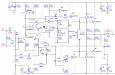
A rough update, just to see if I have it right:
Attachments
Hi,
does it matter where the protection transistor across the VAS goes?
The base monitors the current in the emitter resistor of the VAS (Q4 would need an emitter resistor of about 27r to 30r). The C to E can go either from supply rail to Q4 base or from supply rail to Q13 base.
What difference do these two alternatives make? Are both connections equally effective?
Mjl,
maybe that is your next mod, adding Re to VAS?
Aim for a Vdrop @ quiescent of 200mV to 1000mV, try sim with that range of values. Careful, as you raise VAS Re, the current in Q13 goes up, so you need to make compensating corrections to R27 to maintain the same EF current.
MJL21193 said:
True. Any suggestions for this current control? I can't seem to get the baker clamp to work here - it cuts off the bottom part of the wave at normal levels. I don't know if the cause for this is somewhere else in the circuit.
A rough update, just to see if I have it right:
The simplest solution is the Baker clamp, might you be hitting the reverse breakdown of the diode? Try a 150-200 V low capacitance diode. I'll be out for a bit.
Pete B.
AndrewT said:maybe that is your next mod, adding Re to VAS?
Aim for a Vdrop @ quiescent of 200mV to 1000mV, try sim with that range of values. Careful, as you raise VAS Re, the current in Q13 goes up, so you need to make compensating corrections to R27 to maintain the same EF current.
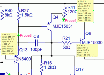
Hi Andrew,
I have added a resistor (r41) shown on the attached pic. Apparently, the current through Q13 was a bit low anyway, for better distortion at higher frequency (distortion at 20Khz has been reduced from .221% to .059% at full output).
Attachments
I have added protection transistor Q16 and this effectively protects the drivers from the high frequency clipping. It has a small impact on the distortion level, just slightly higher.
One thing though is the high amount of current through both Q13 and Q16 while clipping. With 1 VPP overdriven, Q13 goes from 1.7mA (normal) to 60mA (clipping), Q16 goes from 1.1mA (normal) to 42mA (clipping). Is this too much current for these devices to handle? Or, as this is clipping that would normally happen on transients, would it be an issue?
Here's what it looks like:
Attachments
My 50c: Q4 needs emmiter resistor to obtain gain definition in second VAS stage. Second VAS stage has major voltage gain so it needs very good frequency response and stability, therefore you need to cascode Q4 and Q14 for good symmetry (two more transistors with DC base voltage, rail minus 4,7V).
I suggest you choose better type of transistors, like:
Q1, Q2 2SC3381
Q10, Q11 2SA1349
Q4, Q13 2SA1209
Q3, Q14 2SC2911
Q6 2SC5171
Q5 2SA1930
Q9, Q12 2SC5359
Q8, Q7 2SA1987
Also some crucial resistors missing at critical points ... 😀
I suggest you choose better type of transistors, like:
Q1, Q2 2SC3381
Q10, Q11 2SA1349
Q4, Q13 2SA1209
Q3, Q14 2SC2911
Q6 2SC5171
Q5 2SA1930
Q9, Q12 2SC5359
Q8, Q7 2SA1987
Also some crucial resistors missing at critical points ... 😀
Lazy Cat said:...Also some crucial resistors missing at critical points ... 😀
Hi,
Care to elaborate on the above?
These transistors you refer to are very nice. Also hard to find and not presently in my stock. One of the criteria for this design was to use the parts I have.
Each gain stage must have exact load conditions. Emmiter follower of the next stage is current depending load, so you have to ... 
Hi Lazy Cat,
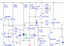
I'm not sure hat you are referring to. Look at this latest schematic and comment in relation to the components on it. For example: put a 5K resistor between Q56 and Q78.
Updated schematic. How many now? Not much similarity between this one and the first one, except the output stage.
I'm not sure hat you are referring to. Look at this latest schematic and comment in relation to the components on it. For example: put a 5K resistor between Q56 and Q78.
Updated schematic. How many now? Not much similarity between this one and the first one, except the output stage.
Attachments
hi MJL21193,
The longer you ask questions the more your schematic will turn into a "standard" schematic found in one of the amplifier design books. At least it is upside down to "normal". 😀
So, can I suggest you have look at R41, I think it should be on the base of Q16. Also, Q17 usually mounts on the main heatsink so it would be better if you selected a device that is easier to mount (e.g. TO220).
If you have a chance, have a look at Carlos's DX HRII design. It is essentailly the same as your's, a Douglas Self/Slone EFII topology with a bootstrap instead of a CCS on the VAS.
regards
Greg Erskine said:..At least it is upside down to "normal". 😀]
Thanks, I think😎
I'm not trying to break new ground here (I certainly don't have enough knowledge and ability for that), just to build a good amp on 56 volt rails with the junk I have laying around.
The TO92 for Q17 won't present a problem for mounting (I'll make a clamp).
If you have a chance, have a look at Carlos's DX HRII design.
I'll do that.
In general, do you believe it is good as is for my needs? Every thing looks good on the simulation - THD, wave shape, voltages and current.
Have I done enough tinkering?
- Status
- Not open for further replies.
- Home
- Amplifiers
- Solid State
- Help with this amp? A patchwork product of simulation