^ This!
And more importantly IMHO, going impedance-balanced removes any shield current flowing between gear from being part of the signalling... mains leakage currents etc out of the picture.
As noted, connecting R36 and C39 bottom legs to an inverter (fed from the output of OP275) instead of GND creates signal-balancing.
Hi folks,
I do appreciate your thinking and input! This is great!
So, let me take a step back and rephrase the rationale behind the project, maybe the solution becomes a lot simpler than I thought so far...
I'm using a DEQX PDC-2.6p digital active cross-over for my active speakers.
Goal is a signal connection avoiding ground signal reference, ground loops and noise pick-up.
One signal connection is made for each of the three ways.of each stereo speaker.
The inputs are equipped with SIA-4.V2 balanced input amps from Funk Tonstudiotechnik (designed for Studio equipment).
The datasheet specifies "4MOhm symmetric" input impedance, max. input voltage 24dBu, CMRR >100dB, CCIR 468/2 qp. noise -98.5dBu
The PDC could generate a balanced or symmetric output with a very expensive add-on board, from the internal unbalanced signals, but that seems technically unnecessary to me in my application without usage of unbalanced connections.
Now as the DAC Chip puts out a differential signal anyway, I thought: Why do all this unbalancing (and other analog stuff I don't use anyway) just to then balance that again? There must be a way to take advantage of the differential signal and directly feed a balanced cable connection.
Firstly I thoght it may be a good idea to use transformers, but this turned out too expensive and seemed techniocally "somewhat inferior", then I checked into AD1853 applications and this lead to where we are now.
If there are parts of the existing and working PDC circuitry which can help achieve balanced output to the balanced inputs, I would appreciate that. If I need to modify or build additional circuitry, that's OK with me.
I hope this helps to set the stage and lead us towards the goal...
Thanks everyone for considering and Regards,
Winfried
Last edited:
Ah!
Forgot a detail of the connection concept: In order to not have lots of cables running/lying around, the idea is to not use bulky XLR stuff, but a cat6 cable connection, with RJ45 sockets built into the PDC and the active speakers. This provides a dedicated pair for each way, plus a Gnd connection, plus one conductor to carry a "remote on/off" signal and the inherent coding comes in handy as well.
Greetings,
Winfried
I have now remeasured the requested points and also corrected the layout analysis result. Please have a look:
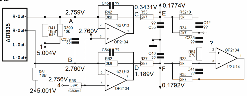
Points E and F seem to still be a good choice to cut and divert the signals for the balanced output buffer.
Regards,
Winfried
Points E and F seem to still be a good choice to cut and divert the signals for the balanced output buffer.
Regards,
Winfried
They are not. Within the passband of the filter, the rightmost op-amp controls away all the differential signal between E and F.
I think this is a more likely schematic:
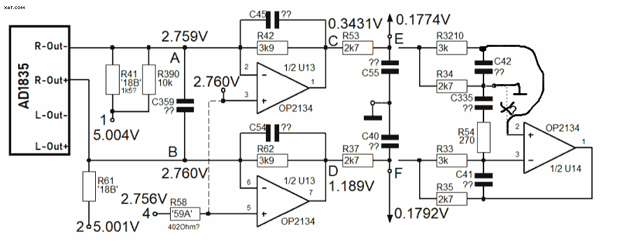
When you either remove R390 or connect an accurate 10 kohm resistor in parallel with R61, you get about equal DC levels at the outputs of U13. C and D are then good points to drive the OPA1632 differential filter stage.
Whether you will need AC coupling between the OPA1632 differential filter stage and your cross-over depends on whether there is DC blocking at the cross-over input. Is there?
By the way, considering it's a digital cross-over, why don't you drive it digitally?
I think this is a more likely schematic:
When you either remove R390 or connect an accurate 10 kohm resistor in parallel with R61, you get about equal DC levels at the outputs of U13. C and D are then good points to drive the OPA1632 differential filter stage.
Whether you will need AC coupling between the OPA1632 differential filter stage and your cross-over depends on whether there is DC blocking at the cross-over input. Is there?
By the way, considering it's a digital cross-over, why don't you drive it digitally?
Last edited:
I would see the following options:
- Use the original unbalanced output but use it balanced: RCA core --> Pin2, RCA shell --> Pin1, RCA shell (+100R breakout) --> Pin3, at the sending end. The 100R breakout is an estimate for impedance balancing, you'd have to trace the output backwards to find the actual resistor value (and mabye a coupling cap which also should then be included in the Pin3 feed). It's not hyper-critical to make the output impedance balanced, though.
- Use the original circuit and find the subtractor output (the last 2134), add couping cap (Nichicon Muse bipolar) -- as there will be DC present -- and breakout R feeding Pin2, and identical network for the Pin3 feed, as above. I would't deal with those I/V input biasing R's (the 1k5 and 1k3 going to 5V) as those are there for a purpose and when made identical we don't know what happens with the downstream signal biasing which might have side effect when not kept in place.
- Remove the 2k7's which go the the subtractor and simply ignore what will happen with the original output. Then use C and D to tap off for your own filter (be it simple copy of dataheet circuit, or extended to superbal as described, or use diff with 1632), then breakout as above (or use the 604R/2n2 final filter as breakout -- though 600R is a bit high resistance). The biasing I would keep in place but make it symmetric (either 1k5 or 1k3 throughout). It is required for biasing the I/V outs close to 0V and the 1k3 gets closer than the 1k5 (without them the DC potential is ~+7V, restricting headroom for the signal swing which then would peak at 10V with that +-0.75mA modulation (which gives 2Vrms at each I/V output). I found out that the DC bias current from the 1853 is a sinking current, not sourcing, as it must be negative for the biasing to work. Actual value would be more like -1.1mA for this part which then would achieve the exact DC levels at C and D that you are measuring.
Last edited:
I really dont have anything to add to the above fantastic and thoughtful help from Marcel and KSTR. My apologies for being a bit absent. We had a severe flooding event here this week, resulting in patchy internet and quite a lot on my mind, plus I got my 3rd booster (feeling a bit cooked/jittery), resulting in my mind simply not being up to detailed analysis of a part i'm not intimately familiar with. I hoped that the hive mind would come through and it certain appears to have.
Yes it does, but only after BAL-SE conversion->PGA volume control->electronic rebalancing. I believe he wants to skip those intermediate stages as he doesnt use the volume control.
Huuuhhh!
Thanks so much for all your reactions! …especially to Klaus, though, for the comprehensive options suggestions!
I‘ll have to thoroughly digest all the info and feedback…
Regarding the OpAmp replacement: Actually, one of my two PDCs has the HD upgrade (using OPA1642s from memory…) incl. the Cap replacement. I‘m currently modifying the non-HD unit, replacing the 2134s in the I-V may be a future option once the balanced outputs work.
On the Qs of understanding:
As I stated earlier, I want to skip unused, unnecessary stages and also avoid to buy the expensive add-on board, which rebalances the interim SE Signals, which fehlt like overkill to me.
I use analog and digital source, then the DSP X-over, then three analog Lines to the balanced pwr amp inputs in the box. A digital Connection would need a digital DSP output add-on board and three DAC circuits per Box which would seem like another Overkill to me…
Best wishes to Inspector for soon recovery from boost and flooding!
I‘ll be back.
Greetings,
Winfried
Last edited:
Hello Klaus and everyone,
did a bit more thinking and it seems that I'd like to go with Klaus' proposal from bullet 3. From what I understood, the resulting schematic would look like this.
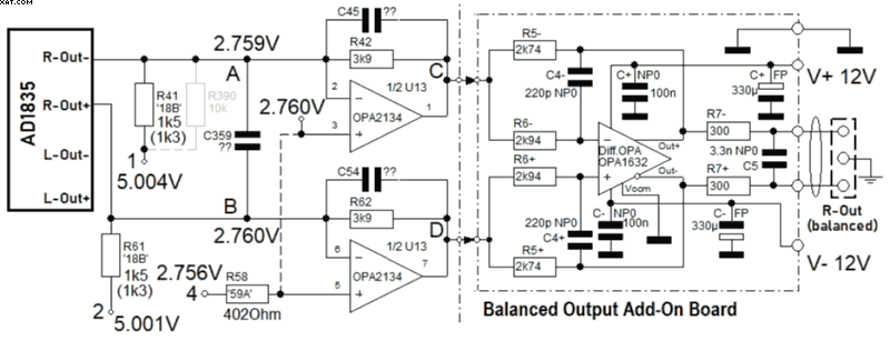
If I'm wrong, kindly suggest corrections 🙂
Regards,
Winfried
did a bit more thinking and it seems that I'd like to go with Klaus' proposal from bullet 3. From what I understood, the resulting schematic would look like this.
If I'm wrong, kindly suggest corrections 🙂
Regards,
Winfried
Marcel,There should be extra RC sections between points C and D and the rest.
sorry, but I feel incompetent to draw what you mean and define the needed values (stated my limited knowledge from the beginning...). A schematic wirh component values would be much appreciated.
Thanks anyway!
Winfried
Hello "rfbrw",Personally, I would forego the frankenfilter and build something from scratch.
same true here as for the former post: I'm sorry, but I feel incompetent to draw/design what you mean, define the needed values and all the rest (I had stated my limited knowledge from the beginning...). A schematic wirh component values would be much appreciated.
Thanks anyway!
Winfried
I mean something like this:
Take the schematic of post #20 and make these changes:
Shift the dashed line to the left, so R53, R37, C40 and C55 become part of the add-on board
Change R37 into 2.74 kohm
Make C40 and C55 equal to 680 pF NP0/C0G
Replace C5 with two 2.2 nF NP0 capacitors to ground
Replace the Cc's with shorts and add coupling caps after the OPA1632 if and only if you need them
Thanks Marcel,
here's Rev. 3 of the balanced Output board.
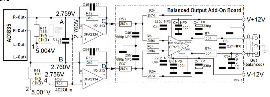
I still have Klaus' suggestions for removing the 10k on my mind and that the 603Ohms for R7+/R7- are on the high side (we have a 4MOhm target device input impedance spec.). What's the suggestion here? The cable length do drive is ~5m.
Thanks for your engaged help!
Winfried
here's Rev. 3 of the balanced Output board.
I still have Klaus' suggestions for removing the 10k on my mind and that the 603Ohms for R7+/R7- are on the high side (we have a 4MOhm target device input impedance spec.). What's the suggestion here? The cable length do drive is ~5m.
Thanks for your engaged help!
Winfried
Twisted pair network cables have a capacitance of about 52 pF/m differential, so 260 pF differential for 5 metres. On top of that, you may have some input RF filter capacitance from the cross-over. 260 pF is not negligible compared to the 2.2 nF/2 = 1100 pF differential of the RC sections at the output, so Klaus has a point.
You can reduce R7 and increase C5 such that the product R7 C5 stays the same. I don't know how far you can go with that, but as the OPA1632 is meant to drive 600 ohm differential loads, halving the resistance and doubling the capacitance should not be a problem.
If you know that the cable is always about 5 metres long, you could also correct for it. For example, take R7 = 300 ohm (or 301 ohm if you prefer E96 values) and C5 = 3.9 nF. The value of C5 is then about 500 pF smaller than it should theoretically be, which compensates for 500 pF/2 = 250 pF differential cable capacitance.
Last edited:
Hi!
5m cable length is planned, 3m may suffice, though, for one of the boxes. The input capacitance is not known, I could ask the vendor for an approximate value. I guess, though, that we're in a good ball park with 5m compensation. The circuit schematic is now tweaked according to accomodate for the cabling.
I'm working on a revised PCB layout: Ceramic Caps require less space with 2.5 of 5mm lead pitch, also went back to direct SOIC8 footprint with supply decoupling SMD Caps on the back side. All other components being through-hole. For the Output Caps I found space for two pcs. in parallel, so I could accommodate for longer cables if needed.
So it seems we are progressing towards a suitable solution 🙂
Greetings,
Winfried
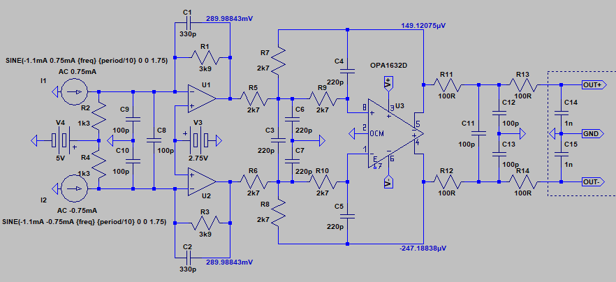
I made a sim to check the 1632 Frankenstein filter, and all looks good.
In a build I'd definitely opt for SMD parts and tight layout (and 4-layer PCB, not a big cost penalty these days), and there are of course many things to consider which are not shown here.
Frequency Response:
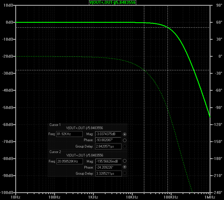
-3dB point: 82kHz, phase at 20kHz: -24deg, magnitude error at 20kHz: -0.2dB. Nominal 0dBFS output voltage is 5.85Vpeak (4.1Vrms).
Increasing the 2k7's to 3k will drop Fc to 75kHz, FWIW.
Time Domain (20kHz):
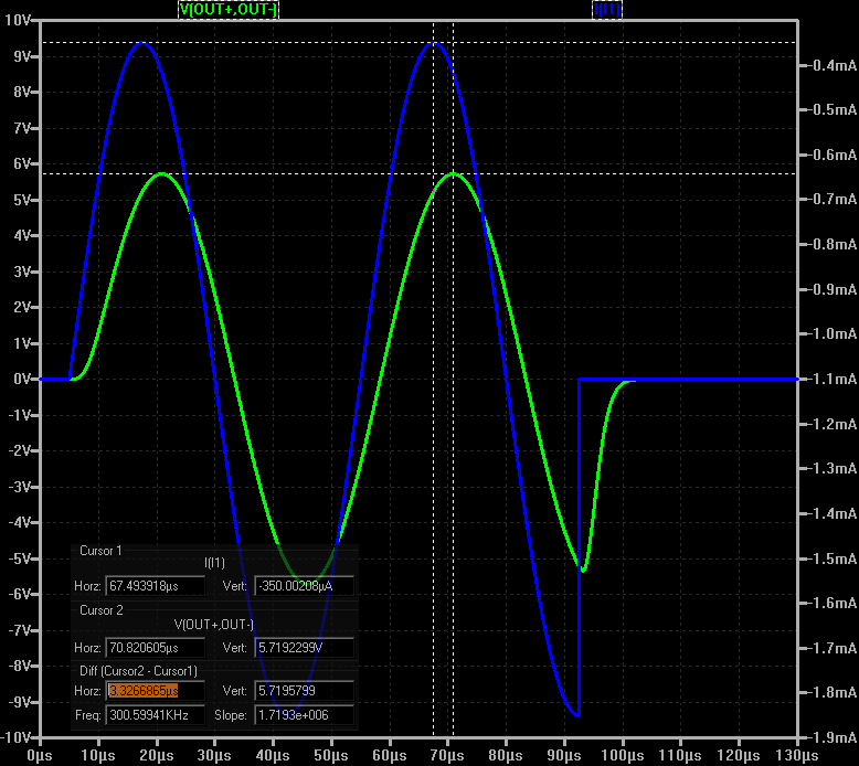
Pretty much optimum, fast settling step response. Total group delay at audio frequencies: ~3.3us.
In a build I'd definitely opt for SMD parts and tight layout (and 4-layer PCB, not a big cost penalty these days), and there are of course many things to consider which are not shown here.
- Those 1nF are worst-case cable + input capacitance check and do not represent 5m of TP network cable. The breakout is made resistive at RF, this also helps to reduce any backfiring RF.
- The filter caps are triples which incorporate some common-mode filtering as well, the equivalent differential capacitance is 1.5x the C value. NP0 5% or better. The triple at the I/V input of course is optional (no mod on the board).
- The resistors are not hyper-critical in absolute value, only matching and tolerance is really important, so 1% or better is basically OK. DC voltage values only shown for reference as they will be different in reality for a number of reasons.
Frequency Response:
-3dB point: 82kHz, phase at 20kHz: -24deg, magnitude error at 20kHz: -0.2dB. Nominal 0dBFS output voltage is 5.85Vpeak (4.1Vrms).
Increasing the 2k7's to 3k will drop Fc to 75kHz, FWIW.
Time Domain (20kHz):
Pretty much optimum, fast settling step response. Total group delay at audio frequencies: ~3.3us.
- Home
- Source & Line
- Digital Line Level
- Help requested: DAC I>V conversion, filter, balanced buffer