Hello DAC experts (which I'm not!),
the motivation for this project comes from the fact that I want to drive my active Speakers' balanced inputs with a balanced Preamp Signal.
The Preamp involved is an old, but well working, DSP DAC PreAmp with 3-Way digital x-overs and equalization capability, working with 24Bit/96kHz resolution, on digital and analog inputs. The standard outputs are cinch connections.
A closer look at the main board shows 18 x OP2134 between the AD1853 DAC Outputs and System's cinch Outputs: The first stages do I>V, filtering and unbalancing, next is analog volume control (PGA2310 based, jumpered "off" because I use digital volume), a jumpered 4 level coarse output control (which I won't need), then a buffer stage for an add-on board (which I don't use) and finally buffers for the cinch outputs (which I won't use an longer...).
So I came to the conclusion (maybe naively?) that I could switch off all circuits the above, cut and derive the signals at the DAC chip outputs and feed them into an own I>V, filtering and balanced output stage made up of just two OPA1632 (fully differential OpAmps) per signal. This would reduce the number of OPAs the signal is fed through to just 2 (one I>V & filter, one as balanced buffer) and have the (just perceived?) advantage to keep signals balanced from the DAC chips' outputs to the balanced Speaker inputs without unbalancing and rebalancing on the way...
After reading AD1853 & OPA1632 vendor application documents and looking at other available I>V/Buffering solutions, I have basically merged two app note schematics into one circuit concept which (I think!) does what's needed.
Here is the AD1853 application from the datasheet:

This is "my" circuit adaptation with OPA1632:

Now I would be very grateful for feedback and input on this, especially on the values chosen for I>V, filtering and buffering, no matter if that's all OK or not OK 😉
Thanks a lot for reading all this.
Best Regards,
Winfried
the motivation for this project comes from the fact that I want to drive my active Speakers' balanced inputs with a balanced Preamp Signal.
The Preamp involved is an old, but well working, DSP DAC PreAmp with 3-Way digital x-overs and equalization capability, working with 24Bit/96kHz resolution, on digital and analog inputs. The standard outputs are cinch connections.
A closer look at the main board shows 18 x OP2134 between the AD1853 DAC Outputs and System's cinch Outputs: The first stages do I>V, filtering and unbalancing, next is analog volume control (PGA2310 based, jumpered "off" because I use digital volume), a jumpered 4 level coarse output control (which I won't need), then a buffer stage for an add-on board (which I don't use) and finally buffers for the cinch outputs (which I won't use an longer...).
So I came to the conclusion (maybe naively?) that I could switch off all circuits the above, cut and derive the signals at the DAC chip outputs and feed them into an own I>V, filtering and balanced output stage made up of just two OPA1632 (fully differential OpAmps) per signal. This would reduce the number of OPAs the signal is fed through to just 2 (one I>V & filter, one as balanced buffer) and have the (just perceived?) advantage to keep signals balanced from the DAC chips' outputs to the balanced Speaker inputs without unbalancing and rebalancing on the way...
After reading AD1853 & OPA1632 vendor application documents and looking at other available I>V/Buffering solutions, I have basically merged two app note schematics into one circuit concept which (I think!) does what's needed.
Here is the AD1853 application from the datasheet:
This is "my" circuit adaptation with OPA1632:
Now I would be very grateful for feedback and input on this, especially on the values chosen for I>V, filtering and buffering, no matter if that's all OK or not OK 😉
Thanks a lot for reading all this.
Best Regards,
Winfried
A problem I see is that your circuit doesn't force a common mode voltage of VREF at the DAC output. Maybe it suffices to connect the VOCM pin of the first differential amplifier to the reference voltage output of the DAC, maybe not. When you do that, then if and only if the DAC DC common mode output current is zero (I think it is, but I'm not entirely sure), you get the correct DC voltage at the DAC outputs, but the common mode impedance is still higher than in the old circuit. Whether that matters depends on how much common mode rubbish comes out of the DAC.
The time constant of the RC section at the output is two times what it should be, so either halve the resistors, or the capacitor, or use two capacitors to ground.
The first differential amplifier sees a capacitive load of at least two times 330 pF in series, in series with 220 pF. That's 94.285714... pF. Can it handle that?
Last edited:
Marcel. no, VCOM on the opa1632 has no effect on the input common mode voltage, it is used to adjust the output to match the common mode voltage of the ADC chosen (in an ADC input circuit) it wasnt designed for biasing the input to match a DAC output. there is no easy way to do this with opa1632, you would need to bias the input in a different manner. I recommend looking at the app note below. its for THS4551 and PCM1794A, but will give an idea.
Attachments
Last edited:
That being said, if your DAC swings around 0VDC, just make sure the opa1632 power supplies do too.
I know, but there are resistors between the inputs and the outputs, so the input common-mode voltage equals the output common-mode voltage if the DAC has zero common mode output current (neglecting the effect of OPA1632 input bias current).Marcel. no, VCOM on the opa1632 has no effect on the input common mode voltage, it is used to adjust the output to match the common mode voltage of the ADC chosen (in an ADC input circuit) it wasnt designed for biasing the input to match a DAC output.
yeah, I only thought of that after I read this DAC has no centre current to account for; thus making a second post. 🙂
I'm scarred by working with dacs that only run on VCC+ for the last 10 years, so didnt think about that.
regardless, the app note I attached above is the most comprehensive breakdown of opamp based trans-impedance stages ive ever read and has been of great usefulness to me personally; so it is highly recommended reading for anyone approaching it IMO. @wgh52
Especially since it covers the use of fully differential amplifiers like opa1632/THS4XXX
I mistook your recommendation as saying the vcom pin had some effect on the input common mode bias/centre current if one was required. They are fantastic parts, but there are a few gotchas, due to the lack of an exposed non-inverting input pin.
Last edited:
OK, many thanks for the input and discussion!
I'll read the attached app note and try to revise my thinking/circuit as I'm not familiar with the issues raised, but at least interested 😉.
A possible alternative may be to keep the existing first 2124 based I>V stage which seems to have an input reference circuit and sense the signals after these. Due to the mainboard being 4-layer and all SMD, detailed reverse engineering seems hard, though. Apicture of the PCB area - maybe it helps...

BTW: The AD1853 is a fixed circuit part I have to live with.
I'll be back.
Winfried
I'll read the attached app note and try to revise my thinking/circuit as I'm not familiar with the issues raised, but at least interested 😉.
A possible alternative may be to keep the existing first 2124 based I>V stage which seems to have an input reference circuit and sense the signals after these. Due to the mainboard being 4-layer and all SMD, detailed reverse engineering seems hard, though. Apicture of the PCB area - maybe it helps...
BTW: The AD1853 is a fixed circuit part I have to live with.
I'll be back.
Winfried
Just had a quick look at the AD1853 datasheet. page 15, it requires a +2.7V common mode input bias in the IV stage. it has only +VCC. would this not mean it has a centre current to account for?
I don't know, the datasheet isn't very clear about the DC common mode current, but Winfried could measure it. If the DC voltages at the outputs of the first OPA2134 are not close to 2.7 V, there must be a common mode DC current somewhere.
Edit: That's assuming there is no DC current flowing through R41, R61, R75 and R87, though, so you also need to check the DC voltages across those.
Edit: That's assuming there is no DC current flowing through R41, R61, R75 and R87, though, so you also need to check the DC voltages across those.
Last edited:
Yes, that should work.A possible alternative may be to keep the existing first 2124 based I>V stage which seems to have an input reference circuit and sense the signals after these.
OK, I guess its down to you Winfred 🙂 I guess I just assume that the inverting inputs of the opa1632 (it only has inverting inputs) would always be fighting to be at VCC+ -> VEE- /2 and unless biased somehow, this wont match the required 2.7V. Marcel is certainly more experienced than I am, so I would defer to him.
yes, given the unknowns, I would probably just stick with using the existing IV stage, they arent bad chips and it appears well enough laid out. then find a way to bypass the somewhat excessive stages after that and account for the DC at the output. some amps are fine with accepting a balanced input with a common mode bias and just cancel it when summed somewhere; some will not like it at all. if your amp is capacitively coupled, you will have no problem.
yes, given the unknowns, I would probably just stick with using the existing IV stage, they arent bad chips and it appears well enough laid out. then find a way to bypass the somewhat excessive stages after that and account for the DC at the output. some amps are fine with accepting a balanced input with a common mode bias and just cancel it when summed somewhere; some will not like it at all. if your amp is capacitively coupled, you will have no problem.
Thanks! Your answers hint at success posibilities, so I'll keep substitute one OPA1632 by the existing first I>V stage. Actually I have no problem to introduce capacitive coupling "somewhere" in the circuit and will give that a thought too. The primary goal is still to build a balanced output, to use the OPA1632 ist second priotity to that (this just seemed handy as the 1853 provides "differential" outputs already).
Looking at the layout again, I wonder about the functions of C45, C54, C61, C358 on the "output side" of U13. Measuring DC and signal there is probably useful. To measure this I'll have to partly reassemble the system and connect a tone generator. Looks like an interesting next step to take 🙂
Greetings,
Winfried
Last edited:
I guess those are the feedback and input capacitors, equivalent to C46, C47 and C57 in the datasheet application circuit.
@wgh52, your proposed circuit probably won't work as the input nodes need to be biased to the 2.7V reference voltage provided by the AD1853. The AD1853 puts out +1mA DC bias and +-0.75mA signal swing per pin and you have to establish the output common mode voltage so that it forces 2.7V at the input nodes with that 1mA DC bias. See here also, discussing the issue (for a PCM1794): https://www.diyaudio.com/community/...level-from-pcm1794-et-al.239357/#post-3565083 (ignore the first hint, though, or see follwoing posts on this). The required V_OCM for the first 1632 is -4.12V +2.7V = -1.42V as far as I can see.
You could also use the datasheet circuit and extend the filter section to balanced output with a "superbal" circuit, a simple G=-1 inverter feed from the output and its output connecting to the parts that normally go to GND (R36, C39). This also removes CM voltage from the filter opamp (making it a DC voltage). Stability has to be watched for is this is now a composite amp, and for the low RF noise gain of 1 for the master opamp you will need a compensation cap accross the feedback resistor of the inverter.
You could also use the datasheet circuit and extend the filter section to balanced output with a "superbal" circuit, a simple G=-1 inverter feed from the output and its output connecting to the parts that normally go to GND (R36, C39). This also removes CM voltage from the filter opamp (making it a DC voltage). Stability has to be watched for is this is now a composite amp, and for the low RF noise gain of 1 for the master opamp you will need a compensation cap accross the feedback resistor of the inverter.
Last edited:
Hello Klaus and everyone!
Yes, all this seems plausible to me as a non-expert....
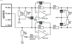
Looking at the existing board layout (as closely as possible...) again, C61 and C53 are obviously supply decoupling. C45 (value unknown) connects to the OP2134 output pin1 (parallel to R42 3.9kOhms) and probably feeds back to the -Input pin2 (under the IC. C54 would then feed Pin 7 back to 6.
Considering all your AD1853 datasheet interpretation, the valuable biasing advice and to keep things simple, I think the safest way to go would be:
So I did some reverse "engineering" of the I>V layout and drew a schematic with what I was able to see/find:
Layout

Schematic

This seems to confirm some of the comments posted previously, although, the SMD- C values are obviously missing and four connections hit vias in the 4 layer board going "god knows where"... Or maybe someone of you can say...? I could measure DC voltages at the quesionmarked points if it helps 🙂
Regards,
Winfried
Yes, all this seems plausible to me as a non-expert....
Looking at the existing board layout (as closely as possible...) again, C61 and C53 are obviously supply decoupling. C45 (value unknown) connects to the OP2134 output pin1 (parallel to R42 3.9kOhms) and probably feeds back to the -Input pin2 (under the IC. C54 would then feed Pin 7 back to 6.
Considering all your AD1853 datasheet interpretation, the valuable biasing advice and to keep things simple, I think the safest way to go would be:
- Keep and use the OP2134 I-V stage (existing on the main board)
- Feed the two I-V output signals (decoupled by Cs)
- Just build the cable connection buffer with an OPA1632 as new external circuit
So I did some reverse "engineering" of the I>V layout and drew a schematic with what I was able to see/find:
Layout
Schematic
This seems to confirm some of the comments posted previously, although, the SMD- C values are obviously missing and four connections hit vias in the 4 layer board going "god knows where"... Or maybe someone of you can say...? I could measure DC voltages at the quesionmarked points if it helps 🙂
Regards,
Winfried
Attachments
Last edited:
Here's a revision of the previous Schematic now including a missed out component:

Well this may answer the biasing question. Please confirm.
Greetings,
Winfried
Well this may answer the biasing question. Please confirm.
Greetings,
Winfried
The resistors with the funny values are probably EIA-96 coded, see https://www.hobby-hour.com/electronics/eia96-smd-resistors.php
Edit: I see you already figured that out.
I wonder why they create an imbalance with the 10 kohm resistors. Maybe the 1.5 kohm resistors compensate for the common mode current, 1 mA per output pin according to KSTR. Otherwise it is all pretty close to the standard application.
Edit: I see you already figured that out.
I wonder why they create an imbalance with the 10 kohm resistors. Maybe the 1.5 kohm resistors compensate for the common mode current, 1 mA per output pin according to KSTR. Otherwise it is all pretty close to the standard application.
Last edited:
Hi Marcel,
thanks for your evaluation! I agree, understanding the rationale behind the 10kOhm resistor would be very interesting, but priority for me is to get the balanced output going 🙂 because the I-V actually works.
Now the connection of the OPA1632 based circuit to the nodes at the right end of the existing circuitry shown needs to be done. To avoid DC issues the use Cs for that connection was recommended. Ultimately I'll cut the traces to the original follow-on circuitry, but now I need to design the Buffer.
Here's my initial idea (I'm sure there are flaws...):

How do I define the coupling Cc value? My rough calculation with 5Hz 6dB/Oct. high pass yielded ~ 20µF which would be physically large when using a mylar Cap (I want to avoid electrolytics in the signal path).
What is everyone's valued advice on Cc value and type?
Regards,
Winfried
thanks for your evaluation! I agree, understanding the rationale behind the 10kOhm resistor would be very interesting, but priority for me is to get the balanced output going 🙂 because the I-V actually works.
Now the connection of the OPA1632 based circuit to the nodes at the right end of the existing circuitry shown needs to be done. To avoid DC issues the use Cs for that connection was recommended. Ultimately I'll cut the traces to the original follow-on circuitry, but now I need to design the Buffer.
Here's my initial idea (I'm sure there are flaws...):
How do I define the coupling Cc value? My rough calculation with 5Hz 6dB/Oct. high pass yielded ~ 20µF which would be physically large when using a mylar Cap (I want to avoid electrolytics in the signal path).
What is everyone's valued advice on Cc value and type?
Regards,
Winfried
- Home
- Source & Line
- Digital Line Level
- Help requested: DAC I>V conversion, filter, balanced buffer