Whereas using a single capacitor cripples common-mode filtering.
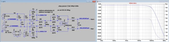
In any case, two times 680 pF in series is 340 pF.
In any case, two times 680 pF in series is 340 pF.
Last edited:
Klaus and Hans! Thanks for the unexpectable simulation work! I'm amazed! And so far as I understand the results, things look well!
I'm a bit concerned about the SMD and 4-layer "mandate", because I understand the electronic and appreciate the size advantages, but am a bit doubtful about my SMD soldering skills and also have not designed a 4-layer board ever...
With Marcel's recommendation/correction to take 340pF instead of 1.36nF, the resulting simulated bandwidth would just be wider and the phase shift lower in the audio band, right?
Now the question is which compromise to take? Better CMRR or better CM-filtering? Two or four layers? SMD or TH? It feels a bit beyond me to make appropriate choices.... Gut feel at the moment: Maybe I could/should do at least a 2-layer SMD board and go with Klaus' schematic seemingly addressing the CMRR and the CM filtering...
Thanks to all!
Winfried
Last edited:
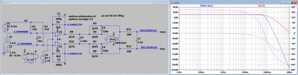
Right, but 340pF gave a bad FR.Whereas using a single capacitor cripples common-mode filtering.
In any case, two times 680 pF in series is 340 pF.
But looking for the flattest possible GD, the optimal value is 680pF.
Hans
Attachments
I favour lossy ceramic bypass caps in these situations. X7R type and as small as you can manually solder, as close to the pins as you can manage.. There is no reason to use NPO there IMO and like films, they can even do harm. fine (good even) for the filter. Honestly I would replace the 330uf with a 2x47uf 1210 ceramic too as well. depends on your power supply though. I'm kind-of anal about symmetry and SMD, so personally I would spend money on susumu thin film 2 part resistor networks over wima films. saves space too and helps with CMRR. but I digress, they arent very easy to find in the values required with the shortages at the moment and the cost for 8 channels may not be economical.
on the capacitive drive capability of opa1632. they actually make a half decent headphone amplifier, even without buffers and I found they drove 300Ω sennheiser quite acceptably, even with a longish cable, so I wouldnt be uber worried about them specifically. I'd worry more about the interaction with the output filter and the amplifier input, but I see you guys are already onto that. You are getting some very high quality help here mate.
on the capacitive drive capability of opa1632. they actually make a half decent headphone amplifier, even without buffers and I found they drove 300Ω sennheiser quite acceptably, even with a longish cable, so I wouldnt be uber worried about them specifically. I'd worry more about the interaction with the output filter and the amplifier input, but I see you guys are already onto that. You are getting some very high quality help here mate.
Regarding X7R decoupling caps, we know they are nonlinear and piezoelectric; they can also be usefully lossy. Also, even low voltage C0G/NPO are a little nonlinear as compared to the higher voltage ones. The problem of course with using highly linear, low-loss caps for decoupling is that they can ring and exhibit sharp impedance variations at or near resonance with themselves and other local components. If one can control for that sort of potential problem, then using linear caps for analog circuit rails can sometimes help with SQ. Helps to have a low capacitance active scope probe to check what's going on.

that would be why I recommended them ... you dont need 'linear' decoupling caps for an opamp, its an oxymoron. the possible ringing, especially in a DAC/DSP unit with a tacked on board, generic 0.1uf value and broken ground plane. not sure where the regulators are going to be? possibly longish connections to those.
They are much more forgiving and there is literally no reason to use NPO for decoupling in this situation IMO. only possible problems
The OP is not experienced at PCB design, does not have much measurement gear (not even sure he has any?). is probably going to go with 2 layer.
Dont muddy the waters for no reason mate.
You get much more benefit being able to shrink the size for the required value and therefore the inductance and X7R allows that. Myself, I would generally try and keep them on the same side as the pin too, rather than connecting to the underside with a via and smaller makes this more doable without interfering too much with the feedback loop and filter routing.
Last edited:
Hello folks,
and thanks for the discussion! So, I will surely take the advice to use 100nF X7R dielectric for supply rail decoupling at the OPA without vias. SMD Rs & Cs will greatly reduce board size and I'll post the board once I'm done, would then welcome improvement feedback.
Yeah! I'm overwhelmed by the patience, good will and quality feedback provided on my project and I learn much more than expected!
Thanks to all!
Winfried
Hello again!
Here's my Rev. 3.2 Schematic:

I hope to have reflected all or most of the suggestions... In any case, I took a go at a dual layer SMD PCB for both L and R channel:
Front side:

Back side ("x-rayed" from front):

All SMDs are 1206 size because that's what my old hands can handle 😉 My Project (just as a friendly reminder) is to have three of these PCBs in the PDC to drive three way active speakers. At the moment there is provision for jumpering the inputs into the Buffer or back to the main board. Not sure if these will stay. Also on the PCB is a muting reed relay to drive the OPA1632 Enable function which shall be driven by the PDCs output muting signal. Still missing are fastening holes as I have to still develop a good way of "piggy backing" the Output Drivers on the main PCB, wanting to keep the cabling from I>V to the Buffer as short as I possibly can...
Greetings,
Winfried
Here's my Rev. 3.2 Schematic:
I hope to have reflected all or most of the suggestions... In any case, I took a go at a dual layer SMD PCB for both L and R channel:
Front side:
Back side ("x-rayed" from front):
All SMDs are 1206 size because that's what my old hands can handle 😉 My Project (just as a friendly reminder) is to have three of these PCBs in the PDC to drive three way active speakers. At the moment there is provision for jumpering the inputs into the Buffer or back to the main board. Not sure if these will stay. Also on the PCB is a muting reed relay to drive the OPA1632 Enable function which shall be driven by the PDCs output muting signal. Still missing are fastening holes as I have to still develop a good way of "piggy backing" the Output Drivers on the main PCB, wanting to keep the cabling from I>V to the Buffer as short as I possibly can...
Greetings,
Winfried
Hi Winfried,
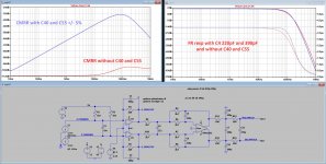
1) Leave C40 and C55, they heavily cripple CMRR as mentioned before, see attachment upper left.
That's exactly where differential topologies shine, the least possible connections to gnd.
2) I have added 260pF at the output for your 5m cable and done the sim again.
Without C40 and C55 and with your latest circuit diagram, your C3 should be 390pF for the flattest possible GD.
Counterintuitive, the larger C3, the further the FR extends, a 1nF value gives the flattest HF response so you have the choice.
3) Since you have an almost empty bottom PCB side, I suggest to use a ground plane.
Hans
Attachments
Hello Hans,
thanks for your valuable input and the simulation effort! Your simulation results look compelling! While technically they point at an electronic optimum, I'm unclear about potential relevance to sound quality - being unable to judge which compromise is best...
on 1.
The choice for having C40 and C55 in the circuit was based on Klaus (kstr) input and simulation results. So, here I'm unsure what to do, but will leave the components on the board to have options.
on 2.
I'll do the same as for 1. and keep the layout to maintain the option of populating or not.
on 3.
Maybe it's not obvious, but the back side already is intended as (kind of) a GND plane. Yes, with a few "cracks". But I hope it will work anyway 😉
Regards,
Winfried
Could be removing C40 and C55 would be over-optimizing the circuit to solve a problem different from the actual problems coming out of the dac. Way to find out is try it both ways, measure, listen, decide which helps most for the particular situation. I don't know why people sometimes seem to want to decide everything in sim or in theory and not by experiment.
Hi Mark,
not sure if I'm the addressee of you remarks... But the way I plan to handle this is, as I wrote, to keep the C40/C55 population option on the board. So the try out path is explicitly open. If I choose to take it is not yet decided, but initially I'll probably leave them out, listen for while, then populate, listen again and if there's no significant or negative subjective difference, I'd leave it as it then is 🙂
@All
the idea came to mind to maybe do some measurements once the circuit works. What these should be would have to be identified... I've got a pretty good Multimeter and a Hameg HM1007 Oscilloscope, the signal/waveform generator would pe a PC application covering audio band frequencies and the signal would be fed into the PDC by koax SPDIF. But all this is potentially for later in the project.
Greetings,
Winfried
Winfried,
To avoid a misunderstanding, the 270pF was just to simulate your 5 m cable capacity, it was not meant to add to your PCB.
Those comments on C40/C55 are showing IMHO a lack of understanding.
Argumentation on what they could possibly add to a differential topology in a positive way would be interesting to hear.
Hans
If they were separated by resistors on each leg then the caps would make more sense. Exactly what AKM did with AK4499 eval board after the I/V. Also, same as what Topping did in D90.
Isn't it obvious? It's nice to have some common-mode filtering because any real-life differential active circuit can generate intermodulation products between the common mode and the differential signals if the common mode signals are large or steep enough. For example, the capacitance of the tail current source of the input differential pair will cause variations of the tail current when the input common mode level changes quickly, which will modulate its differential transconductance.Winfried,
To avoid a misunderstanding, the 270pF was just to simulate your 5 m cable capacity, it was not meant to add to your PCB.
Those comments on C40/C55 are showing IMHO a lack of understanding.
Argumentation on what they could possibly add to a differential topology in a positive way would be interesting to hear.
Hans
In this case it probably doesn't matter much either way: the common-mode rejection is already messed up by the mismatch of the feedback networks of the two transimpedance stages and there is already some common mode filtering in those. My gut feeling is that wgh52 won't measure much of a difference between the circuit with and without C40 and C55, not even if he borrows a fancy audio analyser.
Hi Marcel,Isn't it obvious? It's nice to have some common-mode filtering because any real-life differential active circuit can generate intermodulation products between the common mode and the differential signals if the common mode signals are large or steep enough. For example, the capacitance of the tail current source of the input differential pair will cause variations of the tail current when the input common mode level changes quickly, which will modulate its differential transconductance.
In this case it probably doesn't matter much either way: the common-mode rejection is already messed up by the mismatch of the feedback networks of the two transimpedance stages and there is already some common mode filtering in those. My gut feeling is that wgh52 won't measure much of a difference between the circuit with and without C40 and C55, not even if he borrows a fancy audio analyser.
As always your contribution is highly respected, but isn’t calling the CM/DM IM distortion as an obvious reason to necessitate CM caps a bit far fetched in a differential DAC configuration ?
Fast op-amps can perfectly cope with fast CM signals (spikes) as measured in another thread.
And yes, you are right, the caps around the I/V converter of unknown tolerance and the 220pF caps around the OPA1632 can also negatively affect CMRR.
So, when these 4 caps are of moderate tolerance, the whole CMRR issue is a non issue, almost leading to the question: why differential and not just balanced.
Hans
- Home
- Source & Line
- Digital Line Level
- Help requested: DAC I>V conversion, filter, balanced buffer