The degree of filtering could have to do with progressive insights.Not to Analog Devices's standards.
In the nineties preamps where equipped with tone and loudness control, that's almost a thing of the past now.
NOS Dac's may have opened the eyes concerning the relevance of HF filtering, possibly leading to new insights to some such as Bel Canto.
Analog only produces the D/A converter chip , it's up to the complete converter manufacturer to do what suits him best, maybe in this case less is more 🤔
Hans
No problem at all Hans! yes, there are very good options for hobbyists these days. I sprung first for diptrace middle tier not for profit license about 5 years ago, which allowed 4 signal layers (plus unlimited planes) and 500 pins iirc and that was like $350AUD I think, but upgraded to advanced license middle of last year, which comes with 6 signal layers, 2000 pins unlimited planes and that cost me an additional $250AUD including the upgrade to the latest version; its about half the full price. Ive been using Fusion3D for 3D modelling/CAD for a few years now, with a license that allows me to make a nominal amount from its use; something like 100K. Last year I think it was, after Autodesk acquired EAGLE, they decided to incorporate EAGLE into the suite, so now you can visualise in 3D and incorporate your PCB into your chassis and check clearances, simulate stress points etc (if you buy that plugin). I would love to be able to justify altium and have actually considered doing so for a future project as you can lease a license paying monthly. Nothing else appears to be in the same class that ive seen, but its pricey.
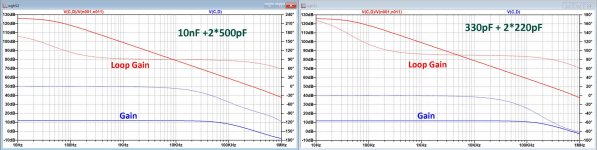
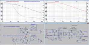
Marcel, since this was an interesting question, I simulated noise and loop gain by using the LT1468 as I/V converter, a fast opamp with 5nV/rtHz, slightly less as the OP275 in Winfrieds A/D converter.A very large capacitor between the virtual ground nodes will increase noise gain and reduce loop gain. Are the noise and distortion performance still reasonable with 10 nF?
The first image shows the loop gain for both versions, indicating that loop gain is not affected by the 10nF.
Concerning noise behavior, I have simulated 4 situations, with first and second order filter around the I/V converters and with and without the filters around the OPA1632.
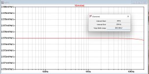
Since all noise spectra were exactly the same, up to two decimals, only one spectrum is shown in the second image.
All this tells nothing about the perceived sound, but technically there are very little differences.
Hans
Attachments
PCB companies say they are getting more and more Kicad submissions from customers. I bought Circuit Studio a few years ago, a crippleware version of Altium. It has some nice features, but not as nice as full blown Altium. With Kicad 6 now out there seems to be no reason not to take advantage of it. Looks like Altium may trying to sell their company; perhaps they see some writing on the wall.
Marcel, since this was an interesting question, I simulated noise and loop gain by using the LT1468 as I/V converter, a fast opamp with 5nV/rtHz, slightly less as the OP275 in Winfrieds A/D converter.
The first image shows the loop gain for both versions, indicating that loop gain is not affected by the 10nF.
Concerning noise behavior, I have simulated 4 situations, with first and second order filter around the I/V converters and with and without the filters around the OPA1632.
Since all noise spectra were exactly the same, up to two decimals, only one spectrum is shown in the second image.
All this tells nothing about the perceived sound, but technically there are very little differences.
Hans
Could you post a schematic, including sources and Spice directives?
Marcel,Could you post a schematic, including sources and Spice directives?
I can imagine very well why you are asking for the sources, because in hindsight I was rather surprised by the noise spectra.
With two 5nV/rtHz I/V converters with 3K9+1K5 around, these resistors producing almost the same amount of noise and with a noise gain of (1+3K9/1K5) per amp, one would expect behind the I/V converters already 1.4(1.4*5nV/rtHz)*(1+3k9/1k5) is ca. 35nV/rtHz.
At the output the OPA1632 circuitry noise would still be added to that, resulting in something slightly above 35nV/rtHz.
Nevertheless it took me some time to find the source of the problem.
The OPA1632 that I used was composed with a universal op-amp, where all relevant parameters were copied from the OPA1632, which always worked without a flaw.
However, just recently LTSpice changed the universal op-amps and as it turned out now, the previous ones are not compatible with the new ones when noise spectra are simulated but for frequency response everything is still O.K., quite weird.
I used an offset voltage of 0.5mV in my sims for this amp, but when changing this offset into 0mV, the whole noise spectrum changed completely, that's how I found out something was no longer compatible.
So, I changed the old universal op-amp for a recent version and everything seems O.K. now.
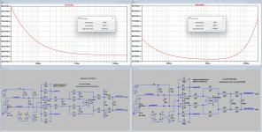
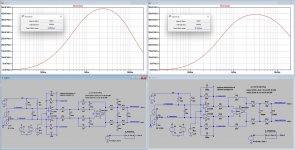
Below in the images you see the difference in noise behavior between the two versions, 330pF+2*220pF and 10nF+2*500pF.
With the 10nF at the input, noise above 10Khz is rising whereas with the 330pF it stays flat.
This results resp in 5.9uV and 7.7uV for the two shown versions, a difference of 2.3dB in favor of the almost single pole version.
When A-weighting these spectra, this reduces to resp 4.7uV and 5.2uV, a difference of only 0.9dB.
I could also have used smaller values like 4.4nF+2*220pF instead of 10nF+2*500pF.
Not shown here, but the unweighted and the weighted noise will then go to resp 5.8uV and 4.3uV, so even below the noise of the 330pF+2*220pF model with its additional filtering.
Keep in mind that this was in no way meant to push anyone in a certain direction, it was just fun to do the sims to get some feeling for differences between the various options.
If you still want the sources, let me know, but I think this noise aspect has been adjusted to where it belonged in the first place.
Hans
Attachments
Last edited:
Hi Klaus and all contributors,
thanks for your thorough analysis and suggestions! Just checked the cost for 4-layer for the same board and found it doubles vs. 2-layer. I may take a go at four layer, but am not certain the bord would be smaller that way.
I have taken the proposal and Installed the Fusion 360 suite. Several hours of becoming familiar with the schematic, sinding the OPA1632 library data and the parts editor, I have a first schematic of my circuit. I did this exercise to have schematic for the layout check I hope to do in the suite. No idea yet how all that works, but that's part of the fun 🙂
Hans,
as a hint on your simulation: The I>V OpAmp in the DEQX system is an OPA2134. Not sure it makes a significant difference, so just for the record.
Regards,
Winfried
Hans, I meant the voltage and current sources, so they are already there. Great that you managed to debug the noise simulation!
How did you simulate the loop gain and is it any different with your new op-amp models?
How did you simulate the loop gain and is it any different with your new op-amp models?
Hi again folks,
Just found out that the private use license version of Fusion 360 is in fact explicitly limited to two (2) layers. My excursion into Fusion may be of use for other, future projects, though. So, 4-layers seems "off" for me, because investing 100s of €s into SW for potentially one project where this would be disable, is not in the budget... 😉
Greetings,
Winfried
Marcel, I only used the op-amp model for the opa1632. For the I/V converters I used the LT1468 which is available in the LTspice library, so this was not affected by the bug.Hans, I meant the voltage and current sources, so they are already there. Great that you managed to debug the noise simulation!
How did you simulate the loop gain and is it any different with your new op-amp models?
To simulate the loop gain, I simulated the FR from 10Hz to 1Mhz and divided the diff output by the diff signal at both virtual ground inputs.
Hans
Last edited:
So why not try Kicad, it’s for free !Hi again folks,
Just found out that the private use license version of Fusion 360 is in fact explicitly limited to two (2) layers. My excursion into Fusion may be of use for other, future projects, though. So, 4-layers seems "off" for me, because investing 100s of €s into SW for potentially one project where this would be disable, is not in the budget... 😉
Greetings,
Winfried
Hans
then try the others, as I said, diptrace free is 2 signal layers plus as many planes as you want (meaning 4 layers is accessible, 2 signal layers, a GND plane and a power plane) and Kicad is free for all versions. I'm running the enterprise/startup license of fusion, but you have to apply for that and not sure if its still available as they changed the pricing structure last year. You have been given many options though, not just that one. You can view more than 2 layers in fusion360 free too btw I think, just cant edit them. I dont typically use it for layout, I use diptrace. just checking it in 3d, so my apologies. You can pay for a month of the whole suite for 53AUD if the 3d stuff is important to you and you can also trial the full featured version for a month for free, so ....
Yes Mark, Kicad looks to be very full featured. I downloaded it, but havent done anything with it as yet. I dont have a fast linux machine to run it in its ideal state anyway. Do you use it on windows @Markw4 ? I only have limited space in my brain for quick keys and these programs are so deep that it does take quite an investment in time to become skilled in all features. I decided i'll stick with diptrace and fusion/eagle until I can justify Altium. The workflow and trace/vector tools in altium along with the realtime 3d routing and multi-board mode; do look like it would pay for itself in time saved fairly quickly, in a professional application anyway.
Last edited:
To simulate the loop gain, I simulated the FR from 10Hz to 1Mhz and divided the diff output by the diff signal at both virtual ground inputs.
Hans
I see. That results in the open loop gain (gain of the op-amp) rather than the loop gain (gain of the op-amp times gain of the feedback network).
There are ways to simulate loop gain including all loading effects using Middlebrook's method, but I never used those (and never understood Middlebrook's method). I'm more familiar with the asymptotic gain model, but that isn't supported by LTSpice.
Marcel, isn't the loop gain circa the open loop gain minus the gain ?I see. That results in the open loop gain (gain of the op-amp) rather than the loop gain (gain of the op-amp times gain of the feedback network).
There are ways to simulate loop gain including all loading effects using Middlebrook's method, but I never used those (and never understood Middlebrook's method). I'm more familiar with the asymptotic gain model, but that isn't supported by LTSpice.
That's why both were shown in the previous images.
But to be more precise since you refer to it, I used both Middlebrook and Tian to get a more accurate result.
In the first image taken to investigate 330pF + 2*220pF, you see the loop gain according to Middlebrook and Tian on top of each other, so both giving exact the same result. Because I only looked at one halve, the 330pF had to be increased to 660pF
At the right you see both open loop gain and gain, where the difference between the two should give circa the same result as both curves at the left.
In the second image I changed the Tian to the equivalent of 10nF, and because it was only halve a section to 20nF.
The Middlebrook version was kept unchanged, but as you see in the image, loop gain is still exactly the same for both, so is the right part of the image compared to the first image.
This all should have shown that 10nF has some effect on noise contribution but has no visible effect on loop gain up to 100Khz.
However as we have seen in another thread, using a MFB filter around the I/V converter had a negative effect on sound perception, most likely because the DAC didn't like the cap directly attached to it's output. So when experimenting, one should listen carefully because nobody knows how the DAC output really looks like internally.
Hans
Attachments

By the way folks: With your deep digging discussion you have actually lost me along the way... I don't understand the criticality regarding the viablity of my project and design at this point. Do I or don't I have a problem? This comment is just for your info, not meant as an offense...
My current roadblock is much simpler (I guess):
I had used KiCAD 5.1 in the past, ran into trouble with missing symbols pretty soon, didn't get a to decent PCB back then, so left it behind in favour of the much less complex layout tool "Sprint".
Well, today I installed KiCAD 6.0.1 and started a new project. Then wanted to insert the OPA1632. And HA! It is not in the 17,000 parts library. Now that's somehow to be expected, in Fusion I had to add it as well, that was straight forward... So, fine, I thought, I have the lib files, let's just do it again!
BUT Haha!: In KiCAD I can't find a way to import symbol / footprint data into a library! The help facility yields no info on such imports! Oh - how I hate having to be an experienced insider to do deadsimple things!
Well anyway: What (the hell!) do I have to do in KiCAD to work with the (missing) OPA1632?
Thanks for sheding light!
Winfried
Last edited:
You might try something like:
https://www.google.com/search?q=opa...57j0i333l2.11622j0j1&sourceid=chrome&ie=UTF-8
https://www.google.com/search?q=opa...57j0i333l2.11622j0j1&sourceid=chrome&ie=UTF-8
surely you know how to create your own parts based on a duplicate of a similar part? you will be able to find a SOIC8 and name the pins appropriately. if you use the MSOP8 pattern/package of the opa1632 (my preference) with the additional heatsink pad, add a 9th pin and connect it appropriately. these are simple tasks that you will come up against at one point or another whichever Application you use.
Last edited:
Making sure you have all needed components in the PCB design software library is the first step even before entering the schematic. It means that you sort of need to have a sketched up schematic and BOM figured out first before doing much if anything in a PCB design program. I typically work it out on paper first.
the information posted has taken the simulation of potential filtering circuits that you may wish to allow for and experiment with the minimum required; they are simulations for narrowing down a couple of options to try perhaps; or at the minimum as an exploration on the topic that will differentiate yours from so many other similar questions. I suggest letting it carry on for a few; as the guys are doing great work.
I always start with a schematic and thus BOM before layout begins; at least rough form. but I always work with scheme and layout linked as a project to allow layouts to be updated based on changes and rule templates etc. occasionally i'll just freestyle a layout, but rarely. usually just as an exploration of form and ideas etc.
you can also check snapEDA and ultralibrarian heres the soic8 opa1632 on ultralibrarian
you can also check snapEDA and ultralibrarian heres the soic8 opa1632 on ultralibrarian
Last edited:
- Home
- Source & Line
- Digital Line Level
- Help requested: DAC I>V conversion, filter, balanced buffer