saturation
Hi Olivier,
>Or is it because a ZENER is more accurate and stable in its voltage?
No, that's not the point. Instead, you need a higher voltage drop in order to protect Qcc1 from saturation.
>If the voltage is wrong why does the simulation still works?
Of course it does work under normal conditions. But look what happens with a too high input voltage (2V or so) and observe Vce of Qcc1. It should never drop below say 0.5V.
Regards,
Edmond.
Lets see, 🙂
2Vin with leds -> Vce qcc1 -> almost goes to 0v (only few millivolts)
same input with 1n4733 zeners -> Vce qcc1 -> keeps AROUND 600mV away from 0v
this proves your claim
the output waveforms are in both cases seriously clipped but apart from that I see no difference. I know sending a Q into SAT is to be avoided unless you use it as a switch but what happens here?
I am obliged to admit that I miss alot of basic knowledge about electronics
doing your test i found out the VCE of Qcc1 is going from about 0v to 2X rail voltage
So the Q's need to have a max VCE of at least the sum of the rail voltages right?
I suppose this is not the case for the output devices of the ops since being in class b they coop only with 1 rail voltage or is it necessary/recommended to use devices specified for twice the rail voltage?
my mosfets are 160V Vds and the rail voltages will be around 80V so this becomes an issue if they need to support 2x80v but my believe is that they need not to be specified for twice the Vcc but just once with quite some reserve off-course...
is this right?
Beste Groeten,
Olivier
Lets see, 🙂
2Vin with leds -> Vce qcc1 -> almost goes to 0v (only few millivolts)
same input with 1n4733 zeners -> Vce qcc1 -> keeps AROUND 600mV away from 0v
this proves your claim
the output waveforms are in both cases seriously clipped but apart from that I see no difference. I know sending a Q into SAT is to be avoided unless you use it as a switch but what happens here?
I am obliged to admit that I miss alot of basic knowledge about electronics
Hi Olivier,
Indeed, many times a sim reveals no difference (because of poor modeling). In real life however, results may less favorable. To be on the safe side, always try to avoid saturation.
doing your test i found out the VCE of Qcc1 is going from about 0v to 2X rail voltage
So the Q's need to have a max VCE of at least the sum of the rail voltages right?
That's right.
I suppose this is not the case for the output devices of the ops since being in class b they coop only with 1 rail voltage or is it necessary/recommended to use devices specified for twice the rail voltage?
my mosfets are 160V Vds and the rail voltages will be around 80V so this becomes an issue if they need to support 2x80v
That's right again. BTW, just simulate the amp and see what happens with Vds.
but my believe is that they need not to be specified for twice the Vcc but just once with quite some reserve off-course...
is this right?
I'm sorry. I have to disappoint you. You will really need 2*Vcc plus some margin.
Beste Groeten,
Olivier
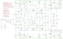
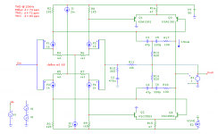
Below my latest revision of the amp. Notice the different voltage clamps. This one monitors Vce of Q25 (respectively Q28). When it gets too low it sources a current via D17, Q15, D13, D7 and finally to the inverting input of the IPS. This way any overloading of any stage is avoided.
Next, see the current limiters, around Q29 and Q30. I have removed the dual slope VI stuff. Although this works fine with a purely resistive load, even a small inductance (i.e. a few meters of speaker wire) makes this kind of limiter highly unstable (because of positive feedback). However, the simple limiter below is not capable to protect the output devices on the 'long run', only for a very short time. Therefore, in case of a short circuit for example, you must add other provisions as well: a relay that disconnects the output from the short. Instead of ordinary diodes for D19 & D20, you might use the diodes of a dual opto-coupler that triggers the additional protection circuitry (these diodes must withstand at least 25mA!)
BTW, if you go on with this circuit, please use my .cir file to start with, as it contains all the AC, DC and transient analysis stuff you need, including thd, ihd and res functions.
Regards,
Edmond.
Attachments
Thnak you Edmond for the circuit.
I did a first look to see the differences between the one I had so far and this new one.
Could you tell me what are the reasons for following alternates?
1)
D4 in your circuit is now below D1 whereas in mine (following your previous hints) it is above D1?
2)
The return lines from collectors Q13/14 go to the diode junction in the input stage or you can say to the collectors of the diff amp Q's whereas in mine it goes back to the mirror Q's?
3) the current sources are simpler, no regulating Q but a zener instead. And the steering resistor R11 is raisond from 100-150 to 1K or more. More stability over temp?
4)
collectors of q17/18 are not to the gnd anymore but have an RC circuit to gnd on one hand and it seems like the same feedback factor circuit on the other hand with nodes labeled c ?
5)
the vas copy Q15 collector at node a goes to gnd via R24 whereas first it also had an RC circuit to gnd in parallel of R24?
6)
collectors q13/14 are tied together with a 1nF cap?
7)
bases of q17/18 are tied together with RC circuit C12R27?
8)
presence d7,10,13,14
9)
there is an RC circuit in the VCC2 powerlines?
10)
the OPS topology baffles me !? is this the principle of 2 bias gens?
11)
one thing i spotted is that the lower bias gen has only 3mA of iq whereas the upperone is around 5mA... is this to compensate Mosfets differences between nchannel and pchannel?
remark : 2sj162 / 2sk1058 surely have Vgs < 0.75V rather 0.65V if i remembered from a measurement you asked me once ....
Could the powerrails be upped to 75V ? I would want at least 250W into 8 ohms ... Vds max of mosfets is 160v
thnx
Olivier
just another remark :
i compared your RS4 analyses with your RS3 ... the thd in the 4th generation is seriously higher than in the 3rd. Why?
i compared your RS4 analyses with your RS3 ... the thd in the 4th generation is seriously higher than in the 3rd. Why?
Below my latest revision of the amp. Notice the different voltage clamps. This one monitors Vce of Q25 (respectively Q28). When it gets too low it sources a current via D17, Q15, D13, D7 and finally to the inverting input of the IPS. This way any overloading of any stage is avoided.
Edmond.
Edmond, can you please post some fourier analysis of yours
amps, since you made some THD simulation ?..
Your designs are fairly well evoluted ,not to say complexes.
It seems to me that such low THD ratios can be reached
with slightly less complexity , while retaining the symetrical
differential topology..
I myself use this topology, with "only" 12 transistors for
the front end , yet , THD is maintained in the 15 ppm rangeAµ
at 20khz/100W/8R..
Both TPC and your beloved TMC give this results.
I will add that TMC is essentially a TPC but with the
great advantage of getting rid of the overshoot that
plague the classical TPC designs..
More to come about it as soon as i ll find a convenient
way of measuring the open loop caracteristics, as classical
tricks don t work with your compensation scheme..
Cheers,
wahab
Edmond, can you please post some Fourier analysis of yours
amps, since you made some THD simulation ?..
Hi wahab,
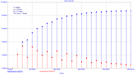
Of course, but due to poor models of lateral MOSFETs, the spectrum is meaningless. Instead, I'll give you the results with vertical MOSFETs, as the models of these trannies (that I have) are far better. See first picture below. Blue = THD, red = IHD (the individual components).
Your designs are fairly well evolved, not to say complexes.
It seems to me that such low THD ratios can be reached
with slightly less complexity , while retaining the symmetrical
differential topology..
I myself use this topology, with "only" 12 transistors for
the front end , yet , THD is maintained in the 15 ppm rangeAµ
at 20khz/100W/8R..
How you did that? Only 12 trannies, yet fully symmetrical + real current sources + beta enhancement trannies + VAS over-current protection + CMCL?

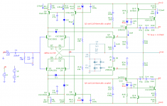
With all above features, I think that the absolute minimum number of trannies is 16, see second picture below. (btw, the DC working point is a little bit critical, hence P1 to adjust the VAS current)
Nevertheless, I like to see your 12 trannies design.
Both TPC and your beloved TMC give this results.
I will add that TMC is essentially a TPC but with the
great advantage of getting rid of the overshoot that
plague the classical TPC designs..
More to come about it as soon as i ll find a convenient
way of measuring the open loop characteristics, as classical
tricks don t work with your compensation scheme..
Cheers,
wahab
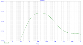
Why you are interested in the open loop response? The behavior/response of feedback loops (global, Miller, voltage clamp, current limiter, you name it) are far more important and/or revealing. In most cases, you have to apply Dr. Middlebrook's method to assess the loop response.
Cheers,
E.
Attachments
Hi wahab,
Of course, but due to poor models of lateral MOSFETs, the spectrum is meaningless. Instead, I'll give you the results with vertical MOSFETs, as the models of these trannies (that I have) are far better. See first picture below. Blue = THD, red = IHD (the individual components).
How you did that? Only 12 trannies, yet fully symmetrical + real current sources + beta enhancement trannies + VAS over-current protection + CMCL?
With all above features, I think that the absolute minimum number of trannies is 16, see second picture below. (btw, the DC working point is a little bit critical, hence P1 to adjust the VAS current)
Nevertheless, I like to see your 12 trannies design.
Why you are interested in the open loop response? The behavior/response of feedback loops (global, Miller, voltage clamp, current limiter, you name it) are far more important and/or revealing. In most cases, you have to apply Dr. Middlebrook's method to assess the loop response.
Cheers,
E.
Thanks for the graphs.
I use hitachi lateral fets models, somewhat sloppy, but
enough to have a general view..
for the schematic, no problem, i ll send it to you by mail soon,
just send me your mail adress in my diy inbox.
There s three stage of voltage amplification, no current
mirror since it would increase complexity without a neat benefit.
Protection of the Vas is a by product of the (simple) design
philosophy.
The VAS itself is an archi classical one, yet it s very rarely
implemented although it reduce THD by 10/20 db compared
to usual designs...
About amps gain , what frightened me is that although
TPC claim a largely higher open loop frequency response,
it seems that as soon as the loop is closed, it has no more
loop gain than TMC.
This lead me to conclude than the two compensation schemes
have intrinsically the same feedback ratios , since the THD
ratios are the same..
Cheers,
wahab
[snip]
About amps gain , what frightened me is that although TPC claim a largely higher open loop frequency response,
I don't know who has said that and in which context, but generally, I think that is not correct.
it seems that as soon as the loop is closed, it has no more loop gain than TMC.
Well, it depends on which loop you are talking about: Miller loop or global loop and equally important, where you have put the 'gain probe' (at the output side, at the inverting input, etc.)
This lead me to conclude than the two compensation schemes have intrinsically the same feedback ratios , since the THD ratios are the same..
Cheers, wahab
In most cases I agree with that. As you know, TPC increases the loop gain of the whole amp, while TMC increases the loop gain as far as the output stage is concerned. As long as the latter is the main culprit of distortion, both methods will show the same reduction in THD.
Cheers,
E.
Well, it depends on which loop you are talking about: Miller loop or global loop and equally important, where you have put the 'gain probe' (at the output side, at the inverting input, etc.)
In most cases I agree with that. As you know, TPC increases the loop gain of the whole amp, while TMC increases the loop gain as far as the output stage is concerned. As long as the latter is the main culprit of distortion, both methods will show the same reduction in THD.
Cheers,
E.
I was talking of course og the global loop.
The miller loop is an inner loop, and as such,
its behaviour is included in the making of the
global loop.
The probe is in the output , since this is there
that the feedback signal is measured by the
amplifier itself.
Your remark about the influence of TPC and TMC
in respect of the amps BW sound right.
Cheers,
wb
Hi Olivier,Thank you Edmond for the circuit.
I did a first look to see the differences between the one I had so far and this new one.
Could you tell me what are the reasons for following alternates?
1)D4 in your circuit is now below D1 whereas in mine (following your previous hints) it is above D1?
In the previous schematics, D1 was put at the wrong position. Now it's okay. Sorry for the confusion
2)The return lines from collectors Q13/14 go to the diode junction in the input stage or you can say to the collectors of the diff amp Q's whereas in mine it goes back to the mirror Q's?
Both configuration are okay, though the latest one is slightly better as it guarantees that D3/D4 are always conducting.
3) the current sources are simpler, no regulating Q but a zener instead. And the steering resistor R11 is raised from 100-150 to 1K or more. More stability over temp?
Indeed, better stability over temperature.
4)collectors of q17/18 are not to the gnd anymore but have an RC circuit to gnd on one hand
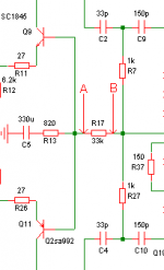
What you see here is a radically different kind of clamp. Instead of feedback to the VAS input (the base of Q17), this one use the inverting input of the IPS as FB point. The actual clamping diodes are D17 and D18. When clamping they transfer the current via Q17 (or Q18) to node C. Q17 and Q18 serve a dual role: as beta enhancement device and as 'serving hatch' for the clamp currents.
and it seems like the same feedback factor circuit on the other hand with nodes labeled c ?
Indeed, same feedback factor (use 1% resistors!). Node C is bootstrapped to the same level as node FB. This way the distortion from the diodes D7, D10, D13 and D14 is minimized.
5)the vas copy Q15 collector at node a goes to gnd via R24 whereas first it also had an RC circuit to gnd in parallel of R24?
6)collectors q13/14 are tied together with a 1nF cap?
7)bases of q17/18 are tied together with RC circuit C12R27?
This time the frequency compensation (by means of C10, C12 and R27) is a bit different, that's all.
8)presence d7,10,13,14
They are part of the clamp and provide a threshold (barrier) between node C and node FB to prevent distortion.
9)there is an RC circuit in the VCC2 power lines?
Yes, in order to improve the PSRR.
10)the OPS topology baffles me !? is this the principle of 2 bias gens?
Indeed, there are two bias generators (Q23 & Q24). They are NOT intended for the OPS, rather for the two totem pole drivers (Q25/Q26 resp. Q27/28). Bias current of the O/P devices is adjusted by means of the 200 Ohms trim pot X1.
11)one thing i spotted is that the lower bias gen has only 3mA of iq whereas the upper one is around 5mA... is this to compensate Mosfets differences between n-channel and p-channel?
The difference (3 vs 5mA) is caused by the currents through Rg3, i.e. 4*0.5mA.
remark : 2sj162 / 2sk1058 surely have Vgs < 0.75V rather 0.65V if i remembered from a measurement you asked me once ....
In that case you can probably delete Rg3.
Could the powerrails be upped to 75V ? I would want at least 250W into 8 ohms ... Vds max of mosfets is 160v
Hmm.. I shouldn't do that. You better stay on the safe side, the more so as this is one of your first projects.
thnx
Olivier
just another remark :
i compared your RS4 analyses with your RS3 ... the thd in the 4th generation is seriously higher than in the 3rd. Why?
Because I've increased the TMC resistors (R33/34) from 470 to 820 Ohms, for better stability.
Cheers,
E.
What's all this global FB stuff, anyhow?
Hi Wahab,
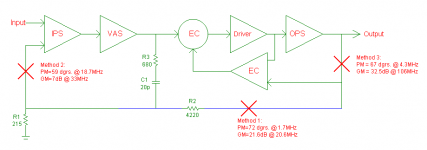
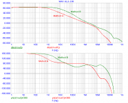
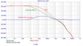
Sometimes things are less than obvious. Also in this case. Clearly you have to put the probe in the return path from output to (inverting) input in order to assess the global FB loop response. BUT... before the TMC resistors or after? Referring to your amp, at point A or B (see 1st picture below).
The 2nd picture depicts the loop response of both methods. As you see they are quite different. I vote for method A.
For an explanation of a similar case (Bob's HEC amp) you might have a look 'over there':
DIY Audio Engineering - Index » Solid-State Design » Power Amplifiers » What's all this global FB stuff, anyhow?
In this case you can even break the loop at three different points and they all give totally different results. As guest you can't see the pictures, but below I've put a copy (3rd pic).
Cheers,
E.
I was talking of course og the global loop.
[snip]
The probe is in the output, since this is there that the feedback signal is measured by the amplifier itself.
[snip]
Cheers,
wb
Hi Wahab,
Sometimes things are less than obvious. Also in this case. Clearly you have to put the probe in the return path from output to (inverting) input in order to assess the global FB loop response. BUT... before the TMC resistors or after? Referring to your amp, at point A or B (see 1st picture below).
The 2nd picture depicts the loop response of both methods. As you see they are quite different. I vote for method A.
For an explanation of a similar case (Bob's HEC amp) you might have a look 'over there':
DIY Audio Engineering - Index » Solid-State Design » Power Amplifiers » What's all this global FB stuff, anyhow?
In this case you can even break the loop at three different points and they all give totally different results. As guest you can't see the pictures, but below I've put a copy (3rd pic).
Cheers,
E.
Attachments
Hi Wahab,
Sometimes things are less than obvious. Also in this case. Clearly you have to put the probe in the return path from output to (inverting) input in order to assess the global FB loop response. BUT... before the TMC resistors or after? Referring to your amp, at point A or B (see 1st picture below).
The 2nd picture depicts the loop response of both methods. As you see they are quite different. I vote for method A.
For an explanation of a similar case (Bob's HEC amp) you might have a look 'over there':
DIY Audio Engineering - Index » Solid-State Design » Power Amplifiers » What's all this global FB stuff, anyhow?
In this case you can even break the loop at three different points and they all give totally different results. As guest you can't see the pictures, but below I've put a copy (3rd pic).
Cheers,
E.
Thank you for the pictured explanations, Edmond.
We differ in the means , since i used an archaic method,
but this end the same way, apparently.
I did break the feedback loop at the point A using a serial
high value ideal inductance as this let the TMC loop
working the way it is supposed to be, i.e , linearizing
the output stage.
I still have some trouble understanding exactly how it works.
The trouble is that although TPC allow for apparent
largely higher loop gain at high frequency , the THD reduction
is no better than TMC in the said frequencies.
cheers,
w
Thank you for the pictured explanations, Edmond.
Hi Wahab,
You're welcome. But did you notice that the 1st picture makes no sense? Beak point B was drawn at the wrong side of the TMC resistors! See below for a correction.
We differ in the means, since i used an archaic method, but this end the same way, apparently.
Not always. If applicable I also use the archaic method. Saves a lot of work, as in MicroCap, Middlebrook's method is a PITA.
I did break the feedback loop at the point A using a serial high value ideal inductance as this let the TMC loop working the way it is supposed to be, i.e , linearizing the output stage.
Okay. So at this point no confusion. (BTW, I first thought that you had put it at position B, as you wrote: 'The probe is in the output'.)
I still have some trouble understanding exactly how it works. The trouble is that although TPC allow for apparent largely higher loop gain at high frequency, the THD reduction is no better than TMC in the said frequencies.
cheers,
w
I fully understand that. Remember Mikeks, who also had serious troubles to understand why and how it works. What is so mystifying about TMC is that if you look at global FB loop gain, you don't see any difference compared to ordinary Miller compensation. This is because the additional loop gain around the OPS is hidden, so to speak. To make it visible you have to break the TMC loop as well, that is, connect the TMC resistors to gnd instead of the output. Hey, you would say, but isn't that TPC? Indeed, that's also TPC and this leads easily to confusion.
Anyhow, one way to assess the additional loop gain is the look at the difference in global loop gain of TPC vs ordinary Miller compensation. See 2nd picture, blue curve. At frequencies of interest it is about 15dB.
For those who are new to this subject: Remember that only the OPS benefits from the extra loop gain instead of the whole amplifier. So why using TMC at all, as TPC gives the same (or maybe even slightly more) reduction in distortion?
First, TPC gives rise to overshoot, which not everybody will appreciate (like me for instance).
Second, TPC increases the VAS loading, which might be another source of distortion.
In contrast, TMC doesn't suffer from these shortcomings.
Cheers,
E.
Attachments
Uh Oh !
Here we have that TPC / TMC story again !
Guys, dont bother selling TPC to Edmond he hates it ;-)
And its probably for the best !
Ciao
Olivier
Here we have that TPC / TMC story again !
Guys, dont bother selling TPC to Edmond he hates it ;-)
And its probably for the best !
Ciao
Olivier
ignore list
I wrote: For those who are new to this subject:...............
BTW, I didn't expect such a comment from someone like you.
Uh Oh !
Here we have that TPC / TMC story again !
I wrote: For those who are new to this subject:...............
BTW, I didn't expect such a comment from someone like you.
Hi Wahab,
What is so mystifying about TMC is that if you look at global FB loop gain, you don't see any difference compared to ordinary Miller compensation. This is because the additional loop gain around the OPS is hidden, so to speak. To make it visible you have to break the TMC loop as well, that is, connect the TMC resistors to gnd instead of the output. Hey, you would say, but isn't that TPC? Indeed, that's also TPC and this leads easily to confusion.
Anyhow, one way to assess the additional loop gain is the look at the difference in global loop gain of TPC vs ordinary Miller compensation. See 2nd picture, blue curve. At frequencies of interest it is about 15dB.
For those who are new to this subject: Remember that only the OPS benefits from the extra loop gain instead of the whole amplifier. So why using TMC at all, as TPC gives the same (or maybe even slightly more) reduction in distortion?
First, TPC gives rise to overshoot, which not everybody will appreciate (like me for instance).
Second, TPC increases the VAS loading, which might be another source of distortion.
In contrast, TMC doesn't suffer from these shortcomings.
Cheers,
E.
HI , Edmond
Agree that TMC has the same intrinsical NFB
than TPC, since the deasappearing OL gain is in fact
due to the use of part of this gain to implement a
local NFB loop comprising the OPS and the VAS, and this
involve that this NFB loop also reduce the VAS THD.
But as connecting the two resistor to ground to display
the OL gain of the VAS + OPS stage, it seems to me
that it s not the good method unless the OPS stage
is orders of magnitude slower than the VAS , as
in this latter case TMC would be almost equal to TPC.
It s better to measure the VAS + OPS OL gain
in insulation by simply breaking the NFB network
whithout changing the ac/dc functionning points and
then dividing the OL gain values by the CL gain values to
have a good idea of the NFB ratios..
Cheers,
w
Last edited:
Edmond,
Don't feel offended. My comment was just meant as a quick practical joke knowing you don't like TPC as we discussed earlier in this thread. I just saw someone 'trying' to sell you TPC and me knowing you don't really like it. But I guess written jokes (just to dedramatize) do not come over as well as told ones since one cannot implement emphasis... The little ;-) eye blinking was for this purpose...
But hey, if you find it misplaced ... I accept ... let's forget it and concentrate on the amp.
Bye Bye
HI , Edmond
Agree that TMC has the same intrinsical NFB than TPC, since the disappearing OL gain is in fact due to the use of part of this gain to implement a local NFB loop comprising the OPS and the VAS, and this involve that this NFB loop also reduce the VAS THD.
Hi Wahab,
You might think that the VAS also benefits from the additional loop gain, as the loop includes the VAS as well. Although the latter is true, the distortion of the VAS is NOT reduced, that is, due to increased loop gain (it is only slightly reduced due to unloading of the VAS output). The reason is that in both cases, ordinary Miller vs TMC, the Miller cap sees (almost) the same voltage, hence the loop gain around the VAS stays the same.
To verify this assertion, I've simulated an amp with ideal components, except of the VAS. This one comprises BJTs without cascodes or 'beta enhancement' trannies. So the VAS is the only component that produces (a lot of) distortion. See 1st figure.
With ordinary Miller compensation (R13/14=820G) THD20k = 74ppm.
With TMC (R13/14=820R) THD20k = 72ppm. Indeed, slightly lower, probably as a result of the unloading effect. But not 15dB lower due to the additional loop gain of TMC.
Strange enough, in case of TPC (R13/14 tied to gnd), THD20k is higher: 83ppm.
But as connecting the two resistor to ground to display the OL gain of the VAS + OPS stage, it seems to me that it s not the good method unless the OPS stage is orders of magnitude slower than the VAS , as in this latter case TMC would be almost equal to TPC.
It s better to measure the VAS + OPS OL gain in insulation by simply breaking the NFB network without changing the ac/dc functioning points and then dividing the OL gain values by the CL gain values to have a good idea of the NFB ratios..
Cheers,
w
After some thoughts I figured out a much simpler way to assess the additional loop gain of TMC; disable the global NFB loop, except for DC, and feed the input signal to the TMC resistors, see 2nd figure. The 3rd graph shows the response of this loop.
Cheers,
E.
Attachments

- Home
- Amplifiers
- Solid State
- HEEEELLLPPP : M. Randy Slone Mirror Image Topology Construction - Troubles