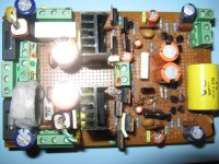
Finished testing with Beta-enhancer, it is stable and predictable. I have designed it as if there is no grounding. The only advantage with that is, it does not clip at all, I have gone high on 4 Ohm test speakers. But it sounds ONLY as good as my reference amp which has IP stage-Cascoded VAS-Driver-OP stage which too neither clips.
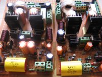
I have tried various pre-VAS circuits even the complex one shown in photo but it provides no benefit neither sounds better then my reference amp. There is only one enhancer I am interested in, hope I finish testing this weekend.
Regards,
Smathias
I have tried various pre-VAS circuits even the complex one shown in photo but it provides no benefit neither sounds better then my reference amp. There is only one enhancer I am interested in, hope I finish testing this weekend.
Regards,
Smathias
Attachments
Hello,
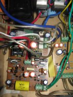
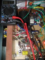
As I was experimenting with simple Beta-enhancer, one of the tiny transistor (mpsa42/92) which protects VAS went bust.
So here was the outcome;
-----------------------------
Voltage at Output: -13V
Voltage at each OP bases: - 31V
Voltage at C & E of Vbe multiplier: High negative something (but 0V across it)
With the driver on the +Vcc side it showed only +4V and on –Vcc it showed -28V
With VAS +31 and -28V
0v at IP
-----------------------------
The above values are as close to what I could remember, though none of the components smoked or ran hot, those are the values I measured quickly. I want to keep my experience short but I would like to point out that troubleshooting would get REAL complex if the amp is not the basic “IP-VAS-Driver-OP” topology.
I have also experienced if there is an impedance mismatch with pre-vas buffer then it can oscillate just one component in the VAS and not at the OP. For now I am keeping beta-enhancer at the last to experiment and will concentrate more with enhancing IP and cascoded VAS. So far whatever I tried with pre-vas the benefits are only less and you don’t really need them if the quality of IP & VAS transistors are not compromised.
Oliver, I have a feeling Edmonds’ ideas would work out fine however try them stage by stage on an already working amp.
You probably need to implement compound pair Vbe multiplier for your amp, it helps to save the base connection and not worry about oscillations if you mount the circuit on the heatsink. When you solder them as one block it turns out rigid and do not twist the C & E cables.
Regards,
Smathias
Attachments
Finished testing with Beta-enhancer, it is stable and predictable. I have designed it as if there is no grounding. The only advantage with that is, it does not clip at all, I have gone high on 4 Ohm test speakers. But it sounds ONLY as good as my reference amp which has IP stage-Cascoded VAS-Driver-OP stage which too neither clips.
I have tried various pre-VAS circuits even the complex one shown in photo but it provides no benefit neither sounds better then my reference amp. There is only one enhancer I am interested in, hope I finish testing this weekend.
Regards,
Smathias
Hello Smathias
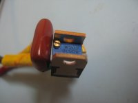
Those insulated fuse holders that you use on the amplifier board can I ask what brand they are.
Regards
Arthur Rappos
Edmond,
I read you are going to go for a cascoded VAS (that makes me happy). Returning on the protection of the VAS. The protection Q can be placed in the Cascode Q or the darlington Q... According to Slone, still, the reason he moves it to the Cascode Q is two ways : 1) eliminate an emitter resistor in the Darlington Q which loads the IS and 2) I don't know exactly, but it has to do with 'soft clipping' protection...
Reason 1 can be dismissed since the CMCL 'needs' an RE at the Darlington Q to operate ... I think? If not necessary I believe it is advized since it reduces temperature drift ...
Reason 2 ? I can't say anything.
I like to see the protection Q on the Cascode Q but again it is merely feeling ...
Could you tell something about the clipping behavior? Comparing both solutions for protecting the VAS??
Yup! Push-pull drivers is going to make me crazy ... I would rather like simple driver stage 🙂 Maybe switching to a more complicated OPS later is possible.
You said something about requiring current to turn the L-Mosfets on... at least talking about full output square wave signal... 100mA peak for a quad stage ... Does it mean our driver stage must have an Iq of >50mA each since there are two? Or does the drivers also work in class B so the Iq can be lower? Are drivers always in class B? Is it a choice?
Bye for now
And euh ... hup holland hup 😉
Edmond,
I read you are going to go for a cascoded VAS (that makes me happy).
Not me
 as it is probably unnecessary to spend four additional trannies. Besides, we both don't like overcomplexity, do we?
 Returning on the protection of the VAS. The protection Q can be placed in the Cascode Q or the darlington Q... According to Slone, still, the reason he moves it to the Cascode Q is two ways : 1) eliminate an emitter resistor in the Darlington Q which loads the IS and 2) I don't know exactly, but it has to do with 'soft clipping' protection...
Reason 1 can be dismissed since the CMCL 'needs' an RE at the Darlington Q to operate ... I think? If not necessary I believe it is advised since it reduces temperature drift ...
Reason 2 ? I can't say anything.
I like to see the protection Q on the Cascode Q but again it is merely feeling ...
First, I suppose you are talking about figure 12.1 in his book, right?
I'm sorry to say so, but Mr Slone (RIP) is wrong. Believe me, it's a serious error.
The preceding EM followers (Q11 & Q12) must be protected as well.
(see also D. Self, that is, his later publications, NOT the one in EW+WW, Feb. 1994, p.139, which is also wrong)
Apart from CMCL issues, eliminating the emitter resistors is also a bad idea, as it will affect the stability of the Miller loop (oscillation around 10...20 MHz or so).
Could you tell something about the clipping behavior? Comparing both solutions for protecting the VAS??
It's not that I'm unfriendly, but I don't like to invest any time into something that is so obviously doomed to a failure. Sorry.
Yup! Push-pull drivers is going to make me crazy ... I would rather like simple driver stage 🙂 Maybe switching to a more complicated OPS later is possible.
Sure, Indeed that's a better idea.
Now we have to look for suitable (more powerful) drivers.
You said something about requiring current to turn the L-Mosfets on... at least talking about full output square wave signal... 100mA peak for a quad stage ... Does it mean our driver stage must have an Iq of >50mA each since there are two? Or does the drivers also work in class B so the Iq can be lower? Are drivers always in class B? Is it a choice?
You don't really need that much quiescent current, as you will never listen to a square wave at full power (besides, your tweeters don't like it either). So a lower Iq is okay as long as the drivers stay in class-A when subjected to a sine of 20kHz at full power, plus some safety margin of course.
Nevertheless, it's common practice to torture an amp with a square wave (funny expression btw, ever seen a wave which is square?) in order to measure the slew rate for example, or to verify/ensure that the amp doesn't show any ringing (measured before the Zobel network!).
Under these exceptional conditions, I don't see why the drivers should still operate in Class-A. If we accept class-AB with regard to the output devices, than why not with regard to the drivers as well?
😀 😀 😀Bye for now
And euh ... hup holland hup 😉
/OT
Did you notice the arrest of the Bavaria girls? Isn't it a bloody shame that the law in South Africa has been changed on behalf of those ******* FIFA bastards?
See: World Cup Marketing Stunt Leads to Arrests - The Lede Blog - NYTimes.com
Groeten, Edmond.
Get me back on track ...
Edmond,
Did you check the 2SA1220 or KSA1220 as drivers? They have the same casing but the Ic is 10x higher, if I remember well, 1A instead of 100mA fot the 2SA1381 or KSA1381. On the other hand they have a lower voltage capability. Around 160V instead of 300V... However if they share the same housing they will both be limited to the more or less the same power limits ?
Anyway, do you like those SA1220? Check them out...
I agree to place the protection Q into the amplifiing Q and thus away from the cascode Q. This leaves us both the choice to incorporate a cascoded vas or not...
Hey Edmond, after listening to Vuvuzela's 😱 for 90 minutes the full power square wave is going to sound like sweet harmony 😀
I will try to reorganize my schematic with the change in protection...
Could you post your latest circuit? Since the push-pull drivers I am a bit lost...😕 I will remake mine too ...
See Ya
Olivier
Hello Guys,
I am glad there is lots of progress on your end and we seem to have started at the same time,
This post is interesting and I have learnt a lot and hope my inputs are also useful.
What Edmond says is true about preceding EM followers (Q11 & Q12) needs protection as well, since I been through so many experiences with pre-vas stage.
My 2 amps are almost complete and last week I have tried out so many configurations with VAS stage including “CASCODING THE CASCODE” and CFP in the VAS stage. This stage was getting so exciting, luckily I fell sick & took off from work and completed experimenting with VAS .
I wanted to try out this idea “CASCODING THE CASCODE” from peufeu’s site;
Memory Distortion Philosophies - Part 5 : Circuits, continued
For a month my amp was already running in cascoded VAS but when I tried “CASCODING THE CASCODE” it sounded dead, I was losing lower bass & higher treble and voltage swing was quite low. Within few hours I decided not to go ahead with this.
I have now lowered cascoded VAS to standard VAS, actually I was in love with cascoded VAS but I found no benefit from it, may be I was not using VAS buffer and not MOSFET Ops.
****I believe if you want real benefit from cacsode VAS then you need to use as VAS buffer and MOSFETS***
CFP in VAS stage was throwing around 3v offset but I have abandoned it for this time as I guess it requires higher value CDOM caps.
Now with standard VAS I don’t have to worry about zener noises in base biasing and voltage swing drops.
I have also removed PRE-VAS simple current buffer and now I don’t have to worry about extra-phase shift issues.
You may try out PRE-VAS current buffer it sounds good!
My thoughts;
If VAS components are not compromised then you don’t need any PRE-VAS stage keeping that IP stage is not de-stabilized at any time by VAS. Will also let you stay away from any phase shift issues.
I tried enhancing Slone’s symmetrical current mirror IP stage with CFP but I couldn’t get it working (maybe I will try again after few months) I am so confident about my amp that I do all test with my real OP BJTs now.
I would have given you the schematic for my amp but I don’t refer to schematics while assembling, I keep everything in my mind and maybe that’s why I don’t end up in errors. (I got this training in my school days and that’s why it is helping me out now )
Regarding Edmonds opinion: “***I don't see why the drivers should still operate in Class-A. If we accept class-AB with regard to the output devices, then why not with regard to the drivers as well?***”
Many (actually me first) will love to use Ops in Class A but that can never be possible with higher power and keeping the SOAR ratings.
I think even the best-Cascoded amplifiers can never match the distortion ratings that of a Class A amplifiers ha ha ha..
If VAS is run at very high quincent Iq then it can cause clipping as it will be hard for the transistors to turn off
Regarding drivers Oliver is there anything simpler than push-pull?
2SA1220 is good but also check 2SC5171
2SA1381 is used for video OP application and it may cause oscillation in audio amps- just my guess
Regards,
Smathias
Attachments
Hello Arthur,
Wow!
i went through "Arthur Rappos gave us a valuable insight into the technicalities of the new formats of SACD and DVDA...."
Those fues holders are from ELCOM - (local product)
Thank God you dint ask about transistors, anyways all npns are duplicates🙂
Regards,
Smathias
Wow!
i went through "Arthur Rappos gave us a valuable insight into the technicalities of the new formats of SACD and DVDA...."
Those fues holders are from ELCOM - (local product)
Thank God you dint ask about transistors, anyways all npns are duplicates🙂
Regards,
Smathias
Hello,
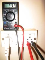
Sometimes the AC voltage in my area shoots up to lethal 330V otherwise it is supposed to be 220V.
When I checked the BIAS volt it is 2.72V for 330V AC
I had actually set the BIAS for 2.4V (But I am not sure about the AC voltage at that time)
My amp is supposed to run with +/- 31V DC but now it is 95.2V DC across !!!!
This amp sits right bang in centre of harsh environment but it does not oscillate or vomit any noise!
I have EI transformers in the North,
Ops on heatsink positioned as antennas to East and West with no grounding.
On the South the fan, now disconnected as this was the most noise maker.
Underground I have AC power & ground cables sneaking.
Inspite of this, there is absolutely no hiss nor hum or any noise generated within the amp as a source of generation!
So far so GOOD!
I am proud of my amp!
Well behaved!!
Regards,
Smathias
Attachments

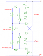
Edmond could you show us a schematic of the push pull driver arrangement you had in mind, I have also experimented a little with this. I once mentioned my experimentations in a thread somewhere and members were thinking I was joking, there is one commercial manufacturer that uses these push pull drivers for mosfets, car amplifiers. A normal JPEG image would do.
Push-pull drivers
Hi Homemodder,
You can do it several ways:
- A diamond buffer.
- A simple push-pull stage biased with a Vbe multiplier.
- Or the most simple one as shown below. Notice that the bias current of the push-pull stages depends on the standing VAS current. So this circuit is only recommended if the latter is well defined and stable.
(Q1 & Q3 respectively Q2 & Q6 are thermally coupled)
Cheers,
E.
@ Olivier: Please be a little patient with me, as I'm also busy with another project.
Attachments
............
I have also experimented a little with this. I once mentioned my experimentations in a thread somewhere and members were thinking I was joking
............
Clearly, those members don't know what they are talking about.
In particular I'm referring to the troubles the ubiquitous 'cross coupled cap' (i.e. the one between the emitters of the drivers) can cause.
Hi
I've come to believe totem pole driving of power mosfet gates is the best way to go. This is the OPS I'm experimenting with now, seems to work quite well, and it also looses that ubiquitous cross coupled cap from gate to gate. I'm using a FMB SOT-6 package monolithic duel comp transistors for A & B. With these fets, the gate to gate voltage is about 7.2V.
I've come to believe totem pole driving of power mosfet gates is the best way to go. This is the OPS I'm experimenting with now, seems to work quite well, and it also looses that ubiquitous cross coupled cap from gate to gate. I'm using a FMB SOT-6 package monolithic duel comp transistors for A & B. With these fets, the gate to gate voltage is about 7.2V.
Attachments
Thanks Edmond, thats about the same ideas Ive tried, they work pretty well, I found the DB to be the best but makes a design too complex. This is the last version I tried in a amp, worked pretty well until I accidently removed the one cap between the output and the base of upper push pull stage, it was critical for stability, at high power the mosfets fried without the cap.
CBS240, thats a interesting outputstage, but just a little bit too complex for my likeing.
CBS240, thats a interesting outputstage, but just a little bit too complex for my likeing.
Attachments
Last edited:
The output Z of the first transistors impede the AC current path from gate to gate of the fets, thus the cap is required or the mosfets will not turn off, will suffer cross conduction and loss of magic smoke. It will be worse the higher frequency you drive.🙂
In regard to my circuit, disregard all the pre-driving HEC circuit, I was pointing out just the part about the driver stage, the drawing is one I posted a while back and no longer have.....computer HD crash.
There is a clamp so as the gates do not overcharge at clipping. This is also rather important in preventing cross conduction. Decoupling caps as close to the drain pins as possible is a good measure for stability as is gate low pass filters.😉 And then there is the bootstrap to make up the voltage taken by Vgs. This way only a few mA is needed for the pre-drivers from the high voltage PS rail and the drivers can still bias 30-40mA. Of course I would never use those outputs if not with EC...🙄 but they have other properties I like very much, such as being tough and costing 69 ; they're very fast and can take high spikes of transient energy.
In regard to my circuit, disregard all the pre-driving HEC circuit, I was pointing out just the part about the driver stage, the drawing is one I posted a while back and no longer have.....computer HD crash.
There is a clamp so as the gates do not overcharge at clipping. This is also rather important in preventing cross conduction. Decoupling caps as close to the drain pins as possible is a good measure for stability as is gate low pass filters.😉 And then there is the bootstrap to make up the voltage taken by Vgs. This way only a few mA is needed for the pre-drivers from the high voltage PS rail and the drivers can still bias 30-40mA. Of course I would never use those outputs if not with EC...🙄 but they have other properties I like very much, such as being tough and costing 69
; they're very fast and can take high spikes of transient energy.
Last edited:
Edmond,
don't worry taking time ... I like football (well soccer for the us dudes which are playing ghana right now ) so i am a bit out of phase for now
but i will be back soon 🙂
just don't leave this project as i need the necessary help because i want to complete this project!!
till later
ghana is up 1 nill dudes ! i forecasted 2-2 at the end of 90min or 120min (just with my colleagues ... )
ciao
time
It's time to pick up the pace guys ! 😉
Vuvuzela's are done with, Tour de France is over, the heatwave in Belgium has passed ... time to do some posting
Well, I must say it is hard to pick up since I lost a bit where we were...
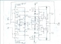
However I guess this schematic comes close to what what supposed to be quite OK.
I just renumbered some components and added a protection circuit against overload and shortcut conditions. DC protection is not incorporated yet (as it will probably be on another PCB)
Especially, Edmond, could you see if there are major goofs?
It is without double bias circuit (push-pull driver stage as you once presented)
It contains cascodes in the VAS which is different from your point of view and protection Q for VAS is hooked on the Cascode Q. When IQVAS causes to drop 0,65V over the VAS current monitor resistor is causes to turn on the protection Q which on his turn closes the cascode transistor shutting down the VAS or limiting its current ... Not sure about its stability behavior.
I also read alot about the ops protection causing stability issues while in protection because the NFB will want to counteract the protections action. This instability is even visible in the simulation when the output load is reduced to 2 ohms or lower ...
I am also a bit lost on the clamp diodes around the VAS !? They protect right ? But what do they protect? What are their main uses?
Greetz for now its sleepy time
It's time to pick up the pace guys ! 😉
Vuvuzela's are done with, Tour de France is over, the heatwave in Belgium has passed ... time to do some posting
Well, I must say it is hard to pick up since I lost a bit where we were...
However I guess this schematic comes close to what what supposed to be quite OK.
I just renumbered some components and added a protection circuit against overload and shortcut conditions. DC protection is not incorporated yet (as it will probably be on another PCB)
Especially, Edmond, could you see if there are major goofs?
It is without double bias circuit (push-pull driver stage as you once presented)
It contains cascodes in the VAS which is different from your point of view and protection Q for VAS is hooked on the Cascode Q. When IQVAS causes to drop 0,65V over the VAS current monitor resistor is causes to turn on the protection Q which on his turn closes the cascode transistor shutting down the VAS or limiting its current ... Not sure about its stability behavior.
I also read alot about the ops protection causing stability issues while in protection because the NFB will want to counteract the protections action. This instability is even visible in the simulation when the output load is reduced to 2 ohms or lower ...
I am also a bit lost on the clamp diodes around the VAS !? They protect right ? But what do they protect? What are their main uses?
Greetz for now its sleepy time
Attachments
It's time to pick up the pace guys ! 😉
Vuvuzela's are done with, Tour de France is over, the heatwave in Belgium has passed ... time to do some posting
Well, I must say it is hard to pick up since I lost a bit where we were...
However I guess this schematic comes close to what what supposed to be quite OK.
I just renumbered some components and added a protection circuit against overload and shortcut conditions. DC protection is not incorporated yet (as it will probably be on another PCB)
Especially, Edmond, could you see if there are major goofs?
It is without double bias circuit (push-pull driver stage as you once presented)
It contains cascodes in the VAS which is different from your point of view
Hi Olivier,
In this particular circuit, a cascode has nothing to offer. Distortion is slightly worse and the max. output voltage is about 3V lower. So why do you insist on using cascodes? Did someone told you to do so?
Besides, even a Hawksford cascode didn't improve the performance.
and protection Q for VAS is hooked on the Cascode Q. When IQVAS causes to drop 0,65V over the VAS current monitor resistor is causes to turn on the protection Q which on his turn closes the cascode transistor shutting down the VAS or limiting its current ... Not sure about its stability behavior.
Please listen to smathias and me. That kind of protection is plain wrong. Instead, you must protect the preceding emitter follower as well. See picture below, Q804 (and/or my file: RS3.CIR).
I also read alot about the ops protection causing stability issues while in protection because the NFB will want to counteract the protections action. This instability is even visible in the simulation when the output load is reduced to 2 ohms or lower ...
Things get better with a decent protection of the VAS. 😀
I am also a bit lost on the clamp diodes around the VAS !? They protect right ? But what do they protect? What are their main uses?
Greetz for now its sleepy time
The clamp diodes limit the excursion of the VAS, i.e. prevent saturation.
But in case of cascodes, you have to replace the LEDs by Zeners (see D802) or even better a voltage reference that provides the same voltage drop as Zcc1.
Regards,
Edmond.
Attachments
Edmond,
I moved the protection as you mentioned. It looks better. When limitting there are no oscillations on the flat (clipped) part of the signal anymore.
For now the cascode is still there, I'll make some simulations with and without it.
As for why I use it? You won't like it... Its like a voodoo thing ;-)
Maybe this glitch in my brain will go away later.
I am going to stay with the clampers too. It sounds good (read : they seem useful).
What I don't get yet is why the LED must be replaced with a ZENER? Supposedly it's about the voltage across 2V for the LED and something 5V for the zener ...
Or is it because a ZENER is more accurate and stable in its voltage?
If the voltage is wrong why does the simulation still works?
Greets,
Olivier
- Home
- Amplifiers
- Solid State
- HEEEELLLPPP : M. Randy Slone Mirror Image Topology Construction - Troubles