Well i put mine into the "largest non used holes" without have to drill or bodge my supply in any way.
FYI - If you don't understand what somebody is trying to explain to you, ask for clarification. #dontbeanasshole
God, you have to love them...
You picked the wrong spots to solder the choke, you Einstein. You picked the dirty/noisy part of the PCB. Do you have any idea how the currents flow on that power supply PCB?
The choke should be soldered where the resistors are soldered - this is where the DC current is clean (after the first C) - no ripple, compared to the spot that you chose which has all the ripple coming straight from the bridge rectifier diodes. Your choice takes the dirty current and feeds it, via the choke, straight to the second C; it's like you omitted the first C.
The other side of the choke is then fed to the entry side of the second C. In this case, you would have a proper CLC that will actually properly reduce the ripple and HF noise, so that you end up with the lowest possible noise figure.
I did not really check what you did with the other side of the choke... my bet is that you also fed the other side of the choke to the wrong side of the second C.

So, the first suggestion by oreo382 did not make any sense to me...his rude comment stunned me... because I could not even imagine that anyone would do what he is suggesting, and what you had actually done.
However, you were both so eager to make a derogative comment when in fact, you have no idea how the chokes should be properly implemented, and how the current feeds to the chokes should be maximised by:
- either using the jumpers
or
- soldering the links thought the resistor eyelets.
Attachments

Last edited:
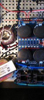
A lovely selection of spots to choose from with larger diameter holes than those for the resistors. There are many I probably missed.
Take your pick. All successful implementations are good. So many options including wire bridges etc. It is DIY after all. Have fun! Be Happy 🙂

Take your pick. All successful implementations are good. So many options including wire bridges etc. It is DIY after all. Have fun! Be Happy 🙂
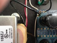
Here are pics of MY build,the one you don't think I own.I can attest my ripple is around 3mv measured with a TRMS Fluke multimter.As far as "dirtiest" place to solder the leads you should try it before making unsubstantiated claims.I can attest there is absolutely NO noise on my build,the "background" is about as black as you can get.By the way,nowhere did I say solder the leads into small resistor holes,I said unused holes as you can see in MY build.
Attachments
Hello Canada,
I see you have some space left to install a choke that will really take it to another level.
Just a few weeks ago my friend changed the 200mH 2,5 A 1ohm chokes in the CLC power supply in the Hiraga i build for him 28 years ago. Now he uses Lundahl LL2771 700mH 2A 2,8!!! ohm. These chokes probably wont fit but you can try LL2733.
The current being used for the stereo amp in my friends amp is close to 2A. When raising the current with 10-15 % the sound goes bad. So you should avoid going over the value in the datasheet.
Greeetings, Eduard
Extreme_Boky - You seem to be in a teaching mood. Could you explain how the points I've circled on the schematic are electrically any different than soldering to the resistor eyelets and to how Oreo382 seems to have implemented theirs? I was planning to do it the same way.
Edited to add, I seem to recall another post where someone wanted to keep the extra resistance from the choke wiring, which could also aid in my implementation.
Edited to add, I seem to recall another post where someone wanted to keep the extra resistance from the choke wiring, which could also aid in my implementation.
I am planning on using the 159zl on my J2 monoblock project and think Extreme_Boky is right about lead locations.
Michael
Michael
I can attest that where I soldered my chokes does not cause noise or anything else.But this is DIY and people can do and believe what they want.
I think we're talking about milli-ohms of resistance difference between one side of the capacitor versus the other side and certainly the much larger resistance of the inductor will override this.
Circuit-wise, the extra resistance is in series with each filter capacitor. The other way, there would be added resistance to the inductor.
pinholer - I think that may have been in reply to my question. Thank you. I still don't quite grasp it, but I'll digest. The "extra" resistance is what I'm hung on.
When I see someone argue (separate from the obvious misunderstandings and name calling) so passionately re: a pro or con to an implementation, I like to understand both sides and see how I can learn about the tradeoffs. To me, wiring/soldering even the smallest loops to the resistor eyelets would (potentially) add more resistance to the circuit vs. the existing traces on the board. However, I'm not sure if that's the difference to which you refer.
More pondering.
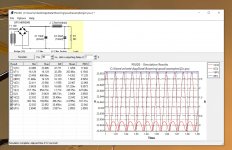
Here is an analysis I made with LTSpice. I used a simple model, but I think that it represents the two scenarios discussed. There is little difference between the two results.
I just wanted to look at the two cases from an analytical viewpoint. Please feel free to comment on the validity of the modelling. I am not an EE and I am always trying to learn more.
I just wanted to look at the two cases from an analytical viewpoint. Please feel free to comment on the validity of the modelling. I am not an EE and I am always trying to learn more.
Attachments

Extreme_Boky - You seem to be in a teaching mood. Could you explain how the points I've circled on the schematic are electrically any different than soldering to the resistor eyelets and to how Oreo382 seems to have implemented theirs? I was planning to do it the same way.
Edited to add, I seem to recall another post where someone wanted to keep the extra resistance from the choke wiring, which could also aid in my implementation.
Compering the schematic diagram, and the PCB layout are two completely different things.
The way you are planning to use the chokes is simply wrong, especially when the PCB is exposed to large constant currents of some 4A give or take an amp. The dirty current will bypass the capacitors (both!), and will flow from the rectifier diodes, through the choke, straight to the AMP PCB's. The micro resistance people are talking here has to be taken within the context of LARGE CURRENTS. These currents will choose the easiest path to go from the rectifier diodes to the short - which is output MOSFETs biased in class A, in this case. The C filtering will do some work, but not really much at all. The capacitors need to see the full 4A current run through their windings, to be able to reduce ripple.
So, the current should run through the first C first, where the ripple will be reduced. THEN, through the choke that will further reduce the mains ripple and HF garbage, AND THEN through the second capacitor, that will filter-out the remainder of the ripple. The power supply PCB has catered for this in its design. This is why the chokes should be connected where the resistors used to be.
The above is basic stuff, anyone who laid out a good PCB design knows this. I started when I was in primary school many decades ago. Then I worked for a company that was making high-quality amplifiers 400W to 2000W (2kW) per side. I helped design them and worked in quality control and optimisation towards achieving better performance. This also included - improvements to the PCB layouts.
Pinholer and Extreme_Boky - Thank you!
A bit of clarification though for my thick head. Staring at the board and the schematic associated with the board for over two hours has done me no good. So, I defer yet again for some help.
Noted. Snipped a bit to save some space.
That all makes perfect sense, but what I'm clearly not grasping is how connecting the choke from (Example) any of the D+ holes to any of the V+ holes is any different from connecting to the holes for (Example) R5. I am clearly missing something, but I never mind posting foolish things if it helps me learn (and possibly someone else, too). I'll take the laughter. 😀
Edited to add - NOW I get it. It always happens as soon as I post. With R5 "missing" it does not work that way. I'll take the dodo award for the day.
Edited again... to show true dodoness.... wait, it should work... I need a
Help!
A bit of clarification though for my thick head. Staring at the board and the schematic associated with the board for over two hours has done me no good. So, I defer yet again for some help.
Compering the schematic diagram, and the PCB layout are two completely different things.
Noted. Snipped a bit to save some space.
So, the current should run through the first C first, where the ripple will be reduced. THEN, through the choke that will further reduce the mains ripple and HF garbage, AND THEN through the second capacitor, that will filter-out the remainder of the ripple. The power supply PCB has catered for this in its design. This is why the chokes should be connected where the resistors used to be.
That all makes perfect sense, but what I'm clearly not grasping is how connecting the choke from (Example) any of the D+ holes to any of the V+ holes is any different from connecting to the holes for (Example) R5. I am clearly missing something, but I never mind posting foolish things if it helps me learn (and possibly someone else, too). I'll take the laughter. 😀
Edited to add - NOW I get it. It always happens as soon as I post. With R5 "missing" it does not work that way.
I'll take the dodo award for the day. Edited again... to show true dodoness.... wait, it should work... I need a
Help!
Last edited:
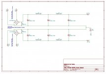
I could not find a great pic, but just in case there is a misinterpretation of what I was getting on about, I made one. This is what I'm talking about. Comparing 1 and 2 to 1a and 2a. Where did I go wrong?! It's got to be something so obvious that I'll hang my head, but now I'm brain fried (clearly).

ItsAllInMyHead, I have no problem interpreting your two scenarios. I guess if we're going to do high resolution analyses, we should also consider the filter capacitor equivalent series resistances.
Thanks Dan and Pinholer.
With Extreme_Boky being so passionate re: using 1 and 2 instead of 1a and 2a - I'm just not clear as to why. Even though they've tried over and over to explain it, it's not gelling. Tomorrow will be another day, and maybe it will click.
Thanks to all for trying.
With Extreme_Boky being so passionate re: using 1 and 2 instead of 1a and 2a - I'm just not clear as to why. Even though they've tried over and over to explain it, it's not gelling. Tomorrow will be another day, and maybe it will click.
Thanks to all for trying.
I could not find a great pic, but just in case there is a misinterpretation of what I was getting on about, I made one. This is what I'm talking about. Comparing 1 and 2 to 1a and 2a. Where did I go wrong?! It's got to be something so obvious that I'll hang my head, but now I'm brain fried (clearly).
View attachment 903983
The capacitors have to be given a chance to conduct a full amount of current (around 4A) AND filter out (short) the ripple to the ground (common)
The incorrectly connected choke will prevent the above from happeneing.
Have a look...
Attachments

- Home
- Amplifiers
- Pass Labs
- Hammond 159zl as clc choke