Fellas, stop simulating!! Build the darn thing and measure the actual noise with incorrectly connected choke, and the with a correctly connected choke.
For the record, I do use chokes in my amp CLC power supplies. I don't use circuit boards but instead hard wire the choke leads directly to the capacitor electrodes. However, I find simulations are great for analyzing circuits and helping me to understand them.
Extreme_Boky - Thank you so much for taking the time to create the graphic. I took a bit of time to digest.
Questions - Isn't the "clean" side the top or output side? Isn't the "dirty" side, the bottom side connected to the diodes? Have I got that a$$-backwards too?
You nailed it, what I'm truly not grasping is different currents flowing (or noise present) on the exact same "hunk of copper" on the board. 1 and 1a are literally on the same "chunk" as are 2 and 2a, I think. I've never explored PCB design. That will need to come later in my exploration and learning.
I think I'll have to stop this journey mid-way and revisit when I get a deeper understanding.
You did not.
The board should be rotated by 180 deg. That is easier than swapping all my comments around 🙂
The board should be rotated by 180 deg. That is easier than swapping all my comments around 🙂
For the record, I do use chokes in my amp CLC power supplies. I don't use circuit boards but instead hard wire the choke leads directly to the capacitor electrodes. However, I find simulations are great for analyzing circuits and helping me to understand them.
Well, by using hard-wiring, you are undeniable telling the current which path it should take. And, this is the best approach.
Your simulations can not capture what I explained in my last photo. A simulation is a great tool, but it does have its limitations. And it seems you found the first big one.
Compering the schematic diagram, and the PCB layout are two completely different things.
The way you are planning to use the chokes is simply wrong, especially when the PCB is exposed to large constant currents of some 4A give or take an amp. The dirty current will bypass the capacitors (both!), and will flow from the rectifier diodes, through the choke, straight to the AMP PCB's. The micro resistance people are talking here has to be taken within the context of LARGE CURRENTS. These currents will choose the easiest path to go from the rectifier diodes to the short - which is output MOSFETs biased in class A, in this case. The C filtering will do some work, but not really much at all. The capacitors need to see the full 4A current run through their windings, to be able to reduce ripple.
So, the current should run through the first C first, where the ripple will be reduced. THEN, through the choke that will further reduce the mains ripple and HF garbage, AND THEN through the second capacitor, that will filter-out the remainder of the ripple. The power supply PCB has catered for this in its design. This is why the chokes should be connected where the resistors used to be.
The above is basic stuff, anyone who laid out a good PCB design knows this. I started when I was in primary school many decades ago. Then I worked for a company that was making high-quality amplifiers 400W to 2000W (2kW) per side. I helped design them and worked in quality control and optimisation towards achieving better performance. This also included - improvements to the PCB layouts.
What is the role of the capacitors in reducing power supply ripple?
The capacitors store electricity. When AC current flows through a rectifier bridge, the AC current with both positive and negative voltage becomes positive voltage. The capacitors store electricity during the peaks of the current flow from the bridge and releases electricity when the current flow is reduced. The more capacitance there is, the smoother the current flows, and voltage fluctuation, or ripple, becomes less.
So in context of the CLC filter, location of the choke connection, and DC ripple, placing a the choke a few millimeters in front of the capacitor does not prevent the capacitor from charging and discharging. It is not the case that there is a continuous flow of DC current through the capacitor and it somehow filters the "dirty current". The capacitor just charges and discharges to fill in the dips.
Attachments
Ben Mah: "It is not the case that there is a continuous flow of DC current through the capacitor and it somehow filters the "dirty current". The capacitor just charges and discharges to fill in the dips."
There is a continuous flow of DC current through the capacitors.
This is exactly why it is important to control the current flow by properly connecting the R (L), and by providing the little indents in the PCB tracks as I have done in the pdf. (Hence, it is better to use hard-wiring in this particular case, as I have already mentioned before).
The current will run through them (capacitors) in the exact same way as the current runs through the choke. The capacitors will decouple the rails by providing a short at ripple frequencies. The chokes will prevent ripple and HF noise by providing high inductance at those frequencies.
The capacitors will store the energy (voltage potential, with the ability to discharge that potential via their ESR). Once the DC potential is stored, the ripple will be decoupled to the common potential (ground). The cleaned-up voltage potential will allow the clean current to flow to the next section of ripple-removal (R or L).
And this can happen only if we force the current down the right path - through the capacitors.
This is exactly why we need to control and separate the dirty current flow, from the cleaned-up current flow.
It takes a while for it to sink in. You also must think of it in a real-time where charging of the capacitors and discharging of that stored energy in a form of current, happens simultaneously whilst the ripple removal is the main goal to be achieved here.
Last edited:
Even if I don't yet understand the "why", I want to make sure I understand Extreme_Boky's explanation. Others seem to be grasping it, I am not.
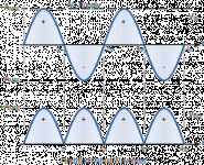
It seems like the statement is that within the same copper pad (is that the correct term?), that the flow of current can be different. We're somehow trying to force the current in a more "correct" and defined way through the choke by using a different set of pads on the same copper plane. I've done a quick job with a hacked color swap to demonstrate what I think is being stated. This is not my contention, it is what I am trying to absorb. So, if I've got it wrong, then I'll once again, just back away.
Instead of everything on the pad behaving "randomly, but the same", each area will behave in some "thoughtful" way from another area based on where they are in relation to other components physically and/or in the chain of the circuit and/or based on board layout. It's given that within a set period of time we have oscillations at different frequencies, otherwise there would be no ripple / noise. Ripple is just (for the sake of this discussion) lower frequency oscillations than "HF" noise. However, it seems that this noise is present at different areas and at varying levels within the same pad. Stated another way, the electrons don't randomly "move about the plane".
So, instead of the red area all having precisely the same characteristics when averaged over a finite period of time, what I think is being stated is that the (randomly chosen in terms of size) pink area behaves differently than the red area, and that the same holds true for the green and light green. Therefore, the choke should be placed correctly onto specific pads within the plane for optimum performance. So, if that is the case, there would seem to be an optimum set of resistor pads based on their placement on the boards.
Which ones and why?
Regardless of whether I understand the "why", is that what is being stated? Is there any literature I can read to grasp this further? It's not fair to ask everyone to keep trying to pound this into me. It's surely in a text somewhere. I hate it when something doesn't sink in. It nags at me.
Thanks for your patience.
I personally think wherever the current goes is not going to matter,there won't be a huge increase in "noise".If someone can show me thru actual meaurements specific to this exact circuit board that there is a difference then go for it.Otherwise don't lose any sleep over wherever you solder your choke.
There is no doubt that there are different results between using the two wiring schemes. The question is what are the magnitudes of the differences. One thing you can do is to wire one channel of the power supply one way and the other the other way and then measure the results. Hands-on experimenting is a good way to help learning. That is why science courses in schools use lab time in addition to lecture time.
As some people say, "The proof of the pudding is in the eating."
As some people say, "The proof of the pudding is in the eating."
Hello,
In the attachment you see the connection of a choke in a CLC configuration in a Hiraga amp i found on a French website. I remember Jean Hiraga telling people to connect the '' output wire '' from the choke in the center of the bar between the last two caps. Not doing this could result in a light bzzz sound sometimes. Probably connecting the choke in the middle of the bar would create an equal situation for both caps. The first one they made had the choke and the circuit itself both connected to the same cap.
However now i read on this French side that there was another connection, I forgot but probably connecting the choke on one cap and the circuit to the other cap.
Anyway with these kind of circuits hard wiring like in the picture would make trying a piece of cake.
Greetings, Eduard
P.s Of course use a serious choke to me 10 mH is a joke once you heard one like in the attachment.
Attachments
I agree wholeheartedly that lab time is critical to application and reinforces understanding. That's my wheelhouse, and I love it. I don't refute there is a difference or even that the magnitude could be meaningful in this application. What I've asked is why the difference exists. Extreme_Boky has provided an explanation. So how do we test it in the lab?
I like to have a proper experimental plan that can clearly lead to a conclusion re: hypotheses. I don't think simply changing the wiring between the two scenarios would lead to a meaningful conclusions to understand the underlying mechanism described by Extreme_Boky. That's predicated on whether I understood their explanation properly, which may not be the case. If I misunderstood, then clearly the underlying research question below would need to be re-worked.
Draft Research Question: "Why does one area within a copper plane or circuit carry current differently (and in a predictable and controllable manner with regard to 'noise') than another area of the same copper plane or circuit when a choke is wired between various points on the plane".
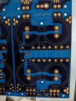
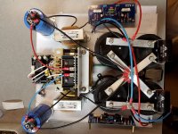
Fixed - Universal PSU V3 power supply board with my current caps, rectifiers, snubber, toroid, AC supply etc. and a Hammond 159ZL.
What independent and dependent variables could be used? What measurements would be most relevant?
A basic DOE may look something like:
A - Point 1 to Point 2 - aka theoretical ideal
B - Point 1a to Point 2a - aka horrible / wrong / not ideal
C - Point 1a to Point 2
D - Point 1 to Point 2a
One could also include various points along the other holes intended for the resistors.
I'd be willing to put in some time and effort vs. just clattering away at a keyboard. I can possibly even learn some new scope functions.
I'll wire the choke to any points specified and take any measurements required within the abilities of my equipment as long as someone can provide the "why" and provide testable hypotheses prior to conducting the experiment. I'm not buying a new scope.
Anyone can correct / amend / add thoughts.
Also, this has become more about me learning than the overall intention of the thread, so if I need to just bail on this, I will. How many angels can dance on a pinhead anyway?
You've all been great. Truly appreciated. It's not that critical that I understand this, but it's fun for me to learn new things. I'm just an old dog trying to learn new tricks and see what ingredients and/or cooking methods have the most effect on the puddings he likes (or doesn't) and why.
Patrick
I like to have a proper experimental plan that can clearly lead to a conclusion re: hypotheses. I don't think simply changing the wiring between the two scenarios would lead to a meaningful conclusions to understand the underlying mechanism described by Extreme_Boky. That's predicated on whether I understood their explanation properly, which may not be the case. If I misunderstood, then clearly the underlying research question below would need to be re-worked.
Draft Research Question: "Why does one area within a copper plane or circuit carry current differently (and in a predictable and controllable manner with regard to 'noise') than another area of the same copper plane or circuit when a choke is wired between various points on the plane".
Fixed - Universal PSU V3 power supply board with my current caps, rectifiers, snubber, toroid, AC supply etc. and a Hammond 159ZL.
What independent and dependent variables could be used? What measurements would be most relevant?
A basic DOE may look something like:
A - Point 1 to Point 2 - aka theoretical ideal
B - Point 1a to Point 2a - aka horrible / wrong / not ideal
C - Point 1a to Point 2
D - Point 1 to Point 2a
One could also include various points along the other holes intended for the resistors.
I'd be willing to put in some time and effort vs. just clattering away at a keyboard. I can possibly even learn some new scope functions.
I'll wire the choke to any points specified and take any measurements required within the abilities of my equipment as long as someone can provide the "why" and provide testable hypotheses prior to conducting the experiment. I'm not buying a new scope.
Anyone can correct / amend / add thoughts.
Also, this has become more about me learning than the overall intention of the thread, so if I need to just bail on this, I will. How many angels can dance on a pinhead anyway?
You've all been great. Truly appreciated. It's not that critical that I understand this, but it's fun for me to learn new things. I'm just an old dog trying to learn new tricks and see what ingredients and/or cooking methods have the most effect on the puddings he likes (or doesn't) and why.
Patrick
I find LTSpice is a very helpful tool. It provides a quick way to test your hypotheses before bringing out the breadboard. Its accuracy, of course, depends on the model that you give it.
As for the model, a simple one will be generally good enough for first order effects. Higher order effects will require adding resistance, capacitance, and inductance which are part of a real build.
As for the model, a simple one will be generally good enough for first order effects. Higher order effects will require adding resistance, capacitance, and inductance which are part of a real build.
Compering the schematic diagram, and the PCB layout are two completely different things.
The way you are planning to use the chokes is simply wrong, especially when the PCB is exposed to large constant currents of some 4A give or take an amp. The dirty current will bypass the capacitors (both!), and will flow from the rectifier diodes, through the choke, straight to the AMP PCB's. .........
I was trying to point out that the capacitors still function and that they are not bypassed.
The capacitors still charge and discharge. The capacitors in conjunction with the choke still act as a filter.
........The current will run through them (capacitors) in the exact same way as the current runs through the choke...........
The choke is in series with the load and the capacitors are parallel to the load. So DC runs through the choke but DC does not run through the capacitors.
I am not disagreeing with the concept of the path taken by the electrons within the copper is important.. I just think that some parts of your explanation may not be clear or persuasive.
I find LTSpice is a very helpful tool. It provides a quick way to test your hypotheses before bringing out the breadboard. Its accuracy, of course, depends on the model that you give it.
No disagreement, but how does a simulation within LTSpice point to the question at hand, which is: "Why do currents potentially flow differently through the same plane of a chunk of copper within a specific board design when one component is connected at various points in the plane?".
Extreme_Boky mentioned specifically that his answers came from his experience in board design.
How do you represent two spots within the same plane within LTSpice? What Extreme_Boky (again if I have not misinterpreted) has stated is that depending on where you put the choke, the current flows differently. Not only that, it seems that depending on that placement, at varying points on the same plane, electrons moving at varying frequencies (Noise / Ripple) are either more or less present and have a propensity to move in a certain way depending on where the choke is placed. He's quite literally stated that one section of the same plane is 'noisier' than another and that by placing one end of the choke further away in physical distance from the rectifiers somehow allows those electrons to choose the caps instead of the choke for their preferred pathway. Literally he said that by placing the choke on a different spot on the plane, that "The dirty current will bypass the capacitors (both!)"bypassed - both sets". How does LTSpice help me understand how/why that occurs? I'm seriously asking. I've read a bit, but I can't get there from here.
As for the model, a simple one will be generally good enough for first order effects. Higher order effects will require adding resistance, capacitance, and inductance which are part of a real build.
Yes, a real build. That's what I'd proposed. I'll do the work, but no one as yet has said what can be actually tested (or simulated) in order to answer the question I'd asked. I'll test, but someone needs to put out a testable hypothesis. I'm stumped. I can't even come up with a theory as to why this phenomena exists other than to visualize waves in a controlled tub of varying dimensions and varying the inlets and outlets. Yes, I know it's not exactly a corollary, but it's a thought.
Others seem to understand it, so I asked for their hypotheses (or better yet facts). I also asked for references to literature. There's no reason to start from scratch on this if it's a known and potentially well-understood phenomenon.
Your answers are very helpful, but from my perspective none deal directly with the question. Or, am I missing something so fundamentally silly that I need to be committed and stop wasting everyone's valuable time?
To be absolutely crystal clear, in case it wasn't, I am not questioning if it occurs, I am asking how/why it occurs. I was advised to bench test, but I can't even imagine how that can be tested. I still gave it a shot re: a DOE. I was advised to simulate to get close, but the simulations won't answer the question (I don't think). We are going in circles.
Again, you guys are awesome for this indulgence, but at some point (which is about now) I have to just need to accept 42 as the answer and move along. Perhaps it will come to me in a dream 😀
Hmmm - solder flux and leaded solder fumes may inspire a thought...

Last edited:
Current will flow along a path of minimum resistance. It could be different between DC and AC. With DC, that would be the shortest path. With AC, capacitive and inductive reactances must be considered.
Adding series resistors to your theoretical design schematic to model the conductor resistances would work for DC analysis. For AC, you would need to also add inductors and capacitors in series/parallel.
However, for the case of investigating these choke wiring schemes, I would first just test the hypothesis that the two schemes produce different results. Wire the power supplies up, add a load to each, and then look at the output. Don't worry about the intermediate nodes at this time. You can use your oscilloscope or use a sound card with software like Room Equalization Wizard to perform FFT analysis. I guess the ultimate would be to power an amp to see if you can hear a difference.
Analyze your results and make your conclusions. Are the differences significant? This may lead to further investigations (form new hypothesis, design experiment, run experiment, analyze results, form conclusions). The Scientific Method is useful for solving many different types of problems.
P.S. In post #92, I show a LTSpice simulation which I attempted to model this situation with added resistors to simulate the extra conductor path. I guess I should do a real world experiment to prove or disprove this model. I've got all the parts to do a point-to-point wired circuit.
Last edited:
- Home
- Amplifiers
- Pass Labs
- Hammond 159zl as clc choke