jcx said:Global loop was disabled for the inner/Gunderson loop gain plot, 10 F kinda pretty sorta effectively shorts out global feedback...
Hi jcx 🙂
I suspect that what you need, in fact, is 10H of inductance, and not capacitance. 🙂
To disable the minor loop while retaining the loading of the global feedback loop, one must first consider that the nominal quantity delivered to the second stage is a current.
To reduce the later quantity to zero, therefore, requires that the second stage (TransImpedance Stage) be inductively decoupled from the first; this 'open-circuits' the connection.
Loop transmission, local to the compensation loop, may then be determined at any point within that loop.
Hi Mikeks,
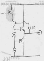
Like this ? Cool 😀
How can we estimate the value of R?
...bias for the 'cascode' device need not be provided by a voltage divider after all....(if a 'non-complementary' TIS is used).
Like this ? Cool 😀
How can we estimate the value of R?
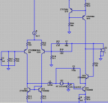
Attachments
Base Ballast Resistor...
Hi Lumanauw 🙂
The value of the base ballast resistor is non-critical (at this stage of my investigation, anyhow); anything from 10R to 100R seems adequate..
lumanauw said:Hi Mikeks,
Like this ? Cool 😀
How can we estimate the value of R?
Hi Lumanauw 🙂
The value of the base ballast resistor is non-critical (at this stage of my investigation, anyhow); anything from 10R to 100R seems adequate..
Mikes,
You don’t have to open all cascaded loops to study the properties of just one, you do need to disable any loop (the Global loop in this case) that encloses the loop studied
You’re still not looking at my circuit – I defeated Global feedback at the frequencies plotted by shorting out the R21,2 Global feedback network - with the ideal controlled current source input stage I've used there is no issue with this approach in my circuit
The quantity I want – as my text has repeatedly explained - is the internal gain of the Q24/Q25,6 composite – when fed by the impedance of the VAS with working Ccm local feedback
The internal loop gain I want to look at is determined by the input impedance – any fair measurement has to include the actual impedance Q24 sees at its emitter in actual circuit operation – which is the output impedance of the VAS with Ccm feedback active
I see you are using different approximations and you’re cutting your loops in different spots – which may well be valid for the perspective you’ve adopted – but I would caution that E2 as output “transistor” very much begs the question of what the Gunderson circuit does – a perfect output stage won’t show any improvement from either “local feedback” or “isolation” of the voltage compliance of Q24 collector at Q25,6 bases – try plotting with a E2 AC error injection term to sim output Vbe error
Jan,
paraphrasing Ed Cherry:
I can think of only 3 ways to linearize a gain stage
Increase the bias to signal ratio - use less of the nonlinear gain curve
Cancellation/predistortion – really only useful with diff pair and push-pull emitter followers, and even order distortions
Negative Feedback – local feedback as in degeneration, emitter/source followers or larger feedback loops including more gain stages
Re: Incidentally...
It would appear, provisionally at least, that this approach is inherently less prone to local parasitic oscillation than Rotel's resistive voltage divider.
I suggest reducing the value of the divider resistors (Rotel's) connected to the output rail by at least 10 to 1 with respect to the resistor connected to each supply rail...
mikeks said:...bias for the 'cascode' device need not be provided by a voltage divider after all....(if a 'non-complementary' TIS is used).
Just connect 'cascode' BJT directly to output rail with a small base ballast resistor...
It would appear, provisionally at least, that this approach is inherently less prone to local parasitic oscillation than Rotel's resistive voltage divider.
I suggest reducing the value of the divider resistors (Rotel's) connected to the output rail by at least 10 to 1 with respect to the resistor connected to each supply rail...
jcx said:I defeated Global feedback at the frequencies plotted by shorting out the R21,2 Global feedback network - with the ideal controlled current source input stage I've used there is no issue with this approach in my circuit...
Hi jcx 🙂
Isn't this a wonderful way to spend a Saturday afternoon? 🙂
It would appear you're trying to establish the loop gain (with frequency) local to Gunderson's network, and NOT the later's impact on the loop transmission of the compensation loop and/or the major loop; is this correct?
[edit: Right - obviously overlapping posts]
I choose to study the distortion reduction claim of the Gunderson “compensation” – you are pursuing AC loop compensation properties – different question - different tools/approximations – overlapping language that has to be intelligently interpreted in each context
To make statements that my analysis is wrong requires understanding and using the same context and language that I am using to illustrate my points
I think over the sum of my posts in this thread there should be little ambiguity about my terms and analysis thrust, just in case:
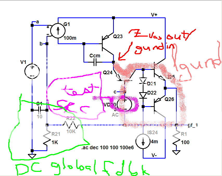
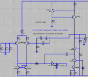
I am interested in the viewpoint that the Gunderson Q24 forms a local feedback loop with the output transistors Q25,6 – “lgund” in drawing
To measure the loop gain of my “lgund” I added a AC test source to VD20 – which is “inside” the “lgund” loop
The loop gain of ”lgund” depends on the impedance at Q24’s emitter – the Q23/Ccm VAS stage
External Global feedback from R21,2/G1 through the VAS would affect the measurement
C1 shorts out R21,2 at the AC frequencies plotted so Spice can establish a DC operating point but there is no feedback V at the inverting input of G1 at tested frequencies
I don’t see any of your objections as valid in this context – care to elaborate?
I choose to study the distortion reduction claim of the Gunderson “compensation” – you are pursuing AC loop compensation properties – different question - different tools/approximations – overlapping language that has to be intelligently interpreted in each context
To make statements that my analysis is wrong requires understanding and using the same context and language that I am using to illustrate my points
I think over the sum of my posts in this thread there should be little ambiguity about my terms and analysis thrust, just in case:
I am interested in the viewpoint that the Gunderson Q24 forms a local feedback loop with the output transistors Q25,6 – “lgund” in drawing
To measure the loop gain of my “lgund” I added a AC test source to VD20 – which is “inside” the “lgund” loop
The loop gain of ”lgund” depends on the impedance at Q24’s emitter – the Q23/Ccm VAS stage
External Global feedback from R21,2/G1 through the VAS would affect the measurement
C1 shorts out R21,2 at the AC frequencies plotted so Spice can establish a DC operating point but there is no feedback V at the inverting input of G1 at tested frequencies
I don’t see any of your objections as valid in this context – care to elaborate?
jcx said:[edit: Right - obviously overlapping posts]
I think so, I was getting a little testy over the communications difficulty
but back pointing to posts on the same page might begin to annoy me again - I hate popping up new windows
Right...
...thanks for clarification, jcx.
In that case your SIM is correct, in principal, as what is required is some means of disabling the global loop (as you've ably indicated) without affecting quiescent conditions.
This then can be established by either using a large capacitor to shunt the inverting input of the input stage to ground (as you've, again, ably indicated); this sets voltage fed back to zero.
Alternatively, as i earlier intimated, the major loop may be disabled by setting the current from the transadmittance (input) stage to the transimpedance stage to zero.
This requires that the connection between the two stages be opened (or decoupled) by inserting a large series inductor between them.
Attachments
Note, however,...
...that while determining the loop gain local to Gunderson's network is undoubtedly stimulating, of far greater relevance, in my humble estimation, is the effect of said network on the loop gains of the major loop and the minor (compensation) loop.
...that while determining the loop gain local to Gunderson's network is undoubtedly stimulating, of far greater relevance, in my humble estimation, is the effect of said network on the loop gains of the major loop and the minor (compensation) loop.
Determining the local Q24/25,6 loop gain is only a part of satisfying my curiosity about whether the local feedback loop perspective on Gunderson’s claimed distortion reduction has any explanatory power
I think it is a useful perspective – but not the only possible view point
If it is useful for distortion reduction then implications for amplifier loop stability have to be addressed
It may be possible that understanding its effect on VAS feedforward zero and other more general loop compensation issues will show it to be (or lead to) better compensation schemes as well that would be useful even in light of the poor distortion reduction performance with already low (Voltage) distortion output stages
Your sim of the “Lgund” loop gain looks broadly similar to my result – within the limits of differing idealizations used – you get a largish low F gain which is probably related to the ratio of VAS Zce to your feedback current source's ouptut Z, where driving the input to your E2 output “Q” isn’t contributing the Q25,6 base impedance load that drags down the low F gain in my sim
thanx
Enjoy the journey
At the end of the day...
...i can only reiterate my earlier observation: Gunderson's compensation is of no discernable practical value.
It reduces major loop transmission at LF-precisely where we need it to increase PSRR, and appears to possess no significant ameliorative impact in respect of HF linearity.
Use double-pole compensation, and live happily ever after..
Bug fix...
In order to maintain the same loop gain for both minor and major loops if, say, the ordinary cascode TIS (without Gunderson's arrangement) is used, then, instead of using the existing common-base transistor to effect Gunderson, an extra transistor, in series with the existing common-base device, must be used.
In order to maintain the same loop gain for both minor and major loops if, say, the ordinary cascode TIS (without Gunderson's arrangement) is used, then, instead of using the existing common-base transistor to effect Gunderson, an extra transistor, in series with the existing common-base device, must be used.
Attachments
This suggests Gunderson's 'output voltage following' device has no effect whatever on the net impedance at the TIS's (so-called VAS) output.
Re: Even so...
It isolates the VAS and Ccm from a non linear voltage at the input of the output stage, as stated in the patent. How much benefit will depend on the impedance of the base of the VAS, the sixe of Ccm, and the type of output stage. I imagine a mosfet output stage would benefit more.
In your last scem there is no output stange, so there will virtually no non linearities at the VAS, so no difference in performance.
At least it's been proved it isn't an error correcting system now.
mikeks said:...of what practical, measurable value is Gunderson's arrangement?
It isolates the VAS and Ccm from a non linear voltage at the input of the output stage, as stated in the patent. How much benefit will depend on the impedance of the base of the VAS, the sixe of Ccm, and the type of output stage. I imagine a mosfet output stage would benefit more.
In your last scem there is no output stange, so there will virtually no non linearities at the VAS, so no difference in performance.
At least it's been proved it isn't an error correcting system now.
jagwap said:It isolates the VAS and Ccm from a non linear voltage at the input of the output stage, as stated in the patent.
Unfortunately, Gunderson's conjecture that shielding the minor-loop from non-linearity at the TIS's output is desirable is, apparently, neither attested in theory nor practice.
In fact, one advantage of minor-loop compensation is that such non-linearity is ameliorated by the local feedback
Exposing the compensation loop to this non-linearity is, therefore, desirable, as evidenced by the fact that Gunderson produces virtually no improvement in linearity.
In other words, with Gunderson, the minor loop is incapable of correcting linearity from which it is needlessly shielded.
This is confirmed in simulation and examination of Rotel's design.
jagwap said:
In your last scem there is no output stange, so there will virtually no non linearities at the VAS, so no difference in performance.
My last schematic was used to demonstrate loop gain only.
- Home
- Amplifiers
- Solid State
- Gunderson compensation..