traderbam said:
Disagree. There is a loop formed by Q24 and the output stage. Q24 emitter sees the output Z of the VAS, which decreases with f.
Yes, but it is not "another" loop, just an alteration of an existing one. And as the Z of the VAS output goes down with frequency Q24 mearly passes that trough to Node 3 like a cascode would. I think this is open to some interpretation, but if concentrate on any minor error correction behaviour, then the original purpose of the circuit as stated in the patent is missed. As Doug Self points out the Ccm capacitor is not the only way to compensate and amp, but the added bonus of local feedback is preferable to just throwing away loop gain at higher frequencies. This circuit has the bonus of not taking that feeback from a very non linear place in voltage terms.
traderbam said:Only if the Q24 Ic is more "mostly constant" than that of the output stage. The Gm linearity of the output stage has the benefit over Q24 as there are two junctions in parallel and emitter degeneration resistors. Not so clear-cut.
Same thing in my book. At least, same in its implications for stability.
So do it. 😎
In the example the current set in the VAS is from a constant curret source, so the only deviation from constant Ic is from the currents required by the output stage drivers. Therefore the base of Q24 can be expected to follow the output a lot more closely than Node 3 where an entire emitter follower stage is switching on and off. These same non linearities apply the the VAS itself.
Amplifiers are not simple, hence the fascination and debate.
jagwap said:[snip]The voltage divider in the Rotel (not seen it. Have a schematic?) will do the same as the zener version but with xdB less feedback (where x is the potential divider ratio, in this case 6dB). [snip]I think a simulation will give more insight.
Are we talking about Q617 in Lumanauw's diagram? I think that one has a completely different function, I think it is the bias regulator. Its E and B are shorted (for AC) to the Vas collector so there is none of the isolation effect.
Jan Didden
janneman said:
Are we talking about Q617 in Lumanauw's diagram? I think that one has a completely different function, I think it is the bias regulator. Its E and B are shorted (for AC) to the Vas collector so there is none of the isolation effect.
Jan Didden
No, it's Q667 & 615, with C617 & 619 as Ccm. The circuit is symetical so has two of these circuits to isolate both VAS's
jagwap said:
No, it's Q667 & 615, with C617 & 619 as Ccm. The circuit is symetical so has two of these circuits to isolate both VAS's
Right.
Did someone say the “S” word?
For a 1st pass I decided to look at Gunderson’s circuit as another compound transistor like Darlington, Sziklai, Baxandall that can be used as “emitter followers”
The plots compare the “gf” compound follower against the single stage versions, with the unbiased complementary follower used to give an extreme example of the Gunderson circuit’s distortion reduction capability
The zero impedance voltage source drive emphasizes the high gain voltage feedback properties, you can investigate current source drive and argue over “local feedback” vs “isolation” but the local feedback explanation/viewpoint works for me
Upper left fft: distortion of zero bias Class B versions exaggerates the distortion due to Vbe dead zone and shows good distortion reduction for Gunderson’s circuit
Upper right fft: distortion of Class A follower show useful distortion reduction for Gunderson’s circuit
In the waveform trace the V(N002,N007) trace is the Q5 ce voltage = the deadzone of the Class B output and the error correction voltage
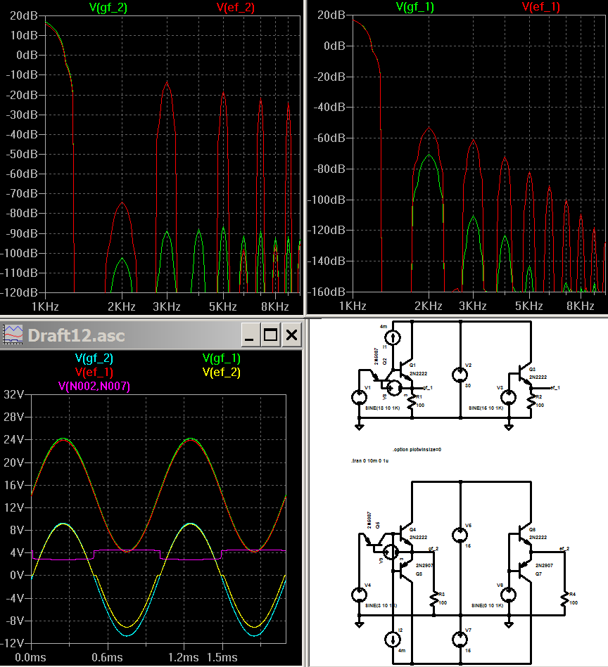
Attachments
Hi, JCX,
Thanks for the effort.
If the strong point of this cct seems not in the "isolation" but in the "local feedback", the difference in the patent (using D20 as fixed value level shifter) and in the practical cct (Rotel=using voltage divider for reference of Q24) may result that the "local feedback" is working or not-working, is it true that using voltage divider is eliminating the merit (=error correcting capabilities) of this cct?
Folks..
As previously noted, it is, perhaps, more useful to consider that, from the perspective of the minor loop, the so-called 'cascode' transistor is merely an emitter follower with respect to voltage fed back from the output stage.
This, indeed, is a negative feedback loop, and conspires to reduce major and minor loop transmission at LF by more than two orders of magnitude.
I suspect that since this loop is considerably degenerative, the magnitude response of the minor loop drops well below unity before output stage singularities compromise minor loop stability.
This, it would appear, is a fascinating way of stifling excess loop transmission whilst nominally enclosing the ouput stage within the monor loop.
However, it is not without obvious vices. For instance, biasing the 'cascode' with a zener diode reference is clearly a faux pas, as the zener will certainly drop-out as the output approaches the rails; Rotels resistive reference slightly ameliorates this problem-methinks
Attachments
Some of what you just wrote might be useful and enlighteneing but I can't really tell. 
Please respond in common tongue.
Conspires? With whom? What transmission are you talking about?This, indeed, is a negative feedback loop, and conspires to reduce major and minor loop transmission at LF by more than two orders of magnitude.
I wouldn't be too sure about that. What do you mean by "singularities" in this context?I suspect that since this loop is considerably degenerative, the magnitude response of the minor loop drops well below unity before output stage singularities compromise minor loop stability.
Yes.However, it is not without obvious vices. For instance, biasing the 'cascode' with a zener diode reference is clearly a faux pas, as the zener will certainly drop-out as the output approaches the rails; Rotels resistive reference slightly ameliorates this problem-methinks
Please respond in common tongue.
JCX, thanks for the simulation. However as there is no VAS, there is no feedback or isolation. Also, in a single ended solution there is little of the distortion worried about to isolate from.
If it is feedback that is of concern then it only works at higher frequencies, as Ccm is the path (and Cobl), and whether it is a level shifter with a gain of 0dB like a zener or a voltage divider as in Rotel then it only alters the amount of feedback. While the zener restricts the headroom of the amplifier earlier than the voltage divider, both of them will hit the VAS unless higher pre-driver rails are used (recommended for lots of other reasons).
However, this circuit is only an error correction system in that it stops an error being passed into the base of Q23 via Ccm, not in the classic sense. So I feel it is misleading to describe it as such.
jagwap said:[snip]While the zener restricts the headroom of the amplifier earlier than the voltage divider, both of them will hit the VAS unless higher pre-driver rails are used (recommended for lots of other reasons).[snip]
... or a simple bootstrap cap combined with the voltage divider?
Jan Didden
Ok...
...this scheme has proved rather disappointing; THD hardly falls by 3dB from 10KHz-20KHz with single-pole miller compensation, and remains completely unchanged at LF.
Double-pole compensation, without Gundersons arrangement, and properly implemented, provides a far more dramatic reduction in nonlinearity.
Was this simulated or on the bench?
Is it possible that it removed more than 3dB, but another THD dominated after it dropped? The patent suggest significanly better results (well it would wouldn't it!)
Is it possible that it removed more than 3dB, but another THD dominated after it dropped? The patent suggest significanly better results (well it would wouldn't it!)
Hi, Janneman,
I also tought that too 😀 But then it turns out that putting bootstrapped on voltage divider towards output node results in the same "stiff" reference like using Zener diode. When output voltage is approaching rail voltage, Q24 will be off when Q23 is turned on, output is not "obeying" Q23.
Hi, Mikeks,
Why you said that? JCX's simulation of this Gunderson using zener (not voltage divider like Rotel) clearly shows that this approach is good.
... or a simple bootstrap cap combined with the voltage divider?
I also tought that too 😀 But then it turns out that putting bootstrapped on voltage divider towards output node results in the same "stiff" reference like using Zener diode. When output voltage is approaching rail voltage, Q24 will be off when Q23 is turned on, output is not "obeying" Q23.
Hi, Mikeks,
Why you said that? JCX's simulation of this Gunderson using zener (not voltage divider like Rotel) clearly shows that this approach is good.
Back to Rotel....
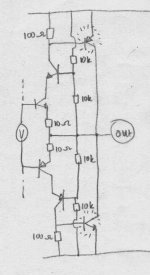
Rotel uses cascode in its input differential. The cascode is voltage divider, towards common emitors, like fig.A.
Other designer uses zener, but towards ground, like fig.B. If the reference is towards ground, Vce of the differential input won't be constant. (like voltage divider in fig.A also not constant Vce)
Is fig.C good? It uses a transistor (base tied to common emitor), zener. Vce of differential input transistor will be constant, and the lower ccs not disturbed (so much) by cascode bias current, because only base attached to common emitor.
Is there any commercial design use fig.C?
jagwap said:Was this simulated or on the bench?
Bench.....with a heavily modified RB1090
jagwap said:The patent suggest significanly better results (well it would wouldn't it!)
'course it would...

lumanauw said:Hi, Mikeks,
Why you said that? JCX's simulation of this Gunderson using zener (not voltage divider like Rotel) clearly shows that this approach is good.
Where?
I haven't commented on JCX's simulation, which, as jagwap has indicated, has nearly nothing to do with Gunderson.
So if Gundersons approach has little benefit and two-pole compensation is much better, we are still left with the mystery why Slone uses a combination of both methods. Could it be the little extra benefit, or is the Gunderson-style approach after all rather there for some other purpose, as has been suggested in earlier threads? Since this wasn't in his book, I don't think he has written anything about it himself, so we probably have to guess his intentions.
janneman said:
... or a simple bootstrap cap combined with the voltage divider?
Jan Didden
I reckon only providing higher supply rails for the voltage gain block would optimise this arragement; otherwise the bootstrap cap. would merely drive the 'cascoded' BJT into cut-off as clip is approached.
Christer said:So if Gundersons approach has little benefit and two-pole compensation is much better, we are still left with the mystery why Slone uses a combination of both methods. Could it be the little extra benefit, or is the Gunderson-style approach after all rather there for some other purpose, as has been suggested in earlier threads? Since this wasn't in his book, I don't think he has written anything about it himself, so we probably have to guess his intentions.
Indeed, i am rather mystified about the practical benefits of this arrangement.
I can send all interested parties a copy of the JAES .pdf; perhaps someone will spot something we've missed.
- Home
- Amplifiers
- Solid State
- Gunderson compensation..