Cathode Resitors
Eldam, I know you will be curious to know the results of the cathode resistor swap. Thank you for your enthusiasm.
I replaced the 220r cathode resistors in the output amplifier. All I can say is WOW! As it was in tuning my amps, upgrading the resistors in the signal path is the single biggest impact. Even more important this early in the signal chain. As good as it was before, this simple upgrade was like the difference between foggy glass and no glass at all in the window. Everything clearer and more dramatic. Particularly important in the higher registers. Bells and cymbals shimmer forever. Air around everything.
Anyone building this circuit is well advised to skip the experiment and go straight to best possible resistors in all 3 positions. Naked foil would be the minimum.
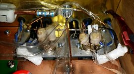
In the pic, the 2 larger white blobs are my I/V resistors built some time ago. The 4 vertical blobs are the new cathode resistors. Basically a piece of bamboo wood with copper wire on each end.. double sided tape around the wood, and Manganin wire bifilar wrapped on the tape and soldered onto the copper leadout. The soldering the wire is the tricky part as it is almost impossible to see even with a magnifying glass. Mostly these things are build by sense of touch! Or just buy the Rhopoint!
Eldam, I know you will be curious to know the results of the cathode resistor swap. Thank you for your enthusiasm.
I replaced the 220r cathode resistors in the output amplifier. All I can say is WOW! As it was in tuning my amps, upgrading the resistors in the signal path is the single biggest impact. Even more important this early in the signal chain. As good as it was before, this simple upgrade was like the difference between foggy glass and no glass at all in the window. Everything clearer and more dramatic. Particularly important in the higher registers. Bells and cymbals shimmer forever. Air around everything.
Anyone building this circuit is well advised to skip the experiment and go straight to best possible resistors in all 3 positions. Naked foil would be the minimum.
In the pic, the 2 larger white blobs are my I/V resistors built some time ago. The 4 vertical blobs are the new cathode resistors. Basically a piece of bamboo wood with copper wire on each end.. double sided tape around the wood, and Manganin wire bifilar wrapped on the tape and soldered onto the copper leadout. The soldering the wire is the tricky part as it is almost impossible to see even with a magnifying glass. Mostly these things are build by sense of touch! Or just buy the Rhopoint!
Attachments
Thanks Wlowes for the review & détails. Have you tried the shematic of Shane above (close to T. Loesch) ?
Does the tubes give you a lot more than solid state with the tda1541(if you tried it with a good scheme before swaping to tubes) ?
@ Ryan,
About the Distinction : Ok I believed the analog ground was only tied to the digital one by pin 5 on the uper side of the vias hole ! I asking myself if the pin 1 to 4 return path ground plane do not see too rapidly pin 5 (analog gnd) instead pin 14 (dgnd) before ? Opportunity to isolate pin 5 by a cut in the top face between pin 4 & pin 5 ! The cut trace will down to pin 14 and up to the edge of the pcb ! pin 28 & 26 will see also pin 14 before the pin 5 if you create an "island tunel trace from the pin 5 to pin 14 by the upper side !
Or is it not important at all... hummm no sure ! this pin 5 is too close to the digital return path like the clock pin if we add a MCLK like the one of Andrea to come !
Would like the advise of Marce about it, but he has few time. I know he likes the continuous gnd plane if a 2 layers design iirc, but this tda 1541 has the agnd and dgnd on the same row and this agnd pin to close to the input digital pins !
What was usefull to have a DGND in the bottom side of the pcb ? Don't remember what we do one year ago when the design was closed !
The idea above is very simple to do with a cutter very carefully ! the most dificult is to the island trace around the upper pin 5 and route it between the 2 rows of 14 vias to the pin 14 : style connected togethers, but pin 5 isolated on the upper side of the curent digital loops which will go easaly to pin 14 first before climbing to pin 5 by the tunel island ! don't know if I am understoodable enough...? No envy to draw something !
At least, no one uses the Johns I2S attenuators with signal diodes he advised (3 in serie for each I2S signal iirc !) ?
regards
Eldam
Last edited:
Thanks Wlowes for the review & détails. Have you tried the shematic of Shane above (close to T. Loesch) ?
Does the tubes give you a lot more than solid state with the tda1541(if you tried it with a good scheme before swaping to tubes) ?
Eldam
I have not tried other tube circuits. Very happy with this one, but I am sure there are many great alternatives. I have not used any good solid state scheme. I could imagine that a Nelson Pass buffer might be quite good. I think if you are a fan of Triodes, I doubt you would be as happy as with this simple tube circuit. I have no urge to make further changes to the analogue side of this beast and am ready to put a top plate on it and leave it alone. 😀
Ah , Shane ask me in PM to ask you if the tantalum resistor are magnetic... and also: UK AUDIO Note resitor and not Japonese Shinkoh ? If I understood him correctly!
I believe you can answer here... Bourn movie symptom : baned and hidden but still reading sometimes all related to tda1541 as he loves this dac chip and tubes for it 🙂
I believe you can answer here... Bourn movie symptom : baned and hidden but still reading sometimes all related to tda1541 as he loves this dac chip and tubes for it 🙂
They are the actual SHINKOH. NOS from Partsconnexion.com $3.45USD ea.
My home made ones left them in the dust. Each resistor took 2 feet of wire to make 224R.
My home made ones left them in the dust. Each resistor took 2 feet of wire to make 224R.
They are the actual SHINKOH. NOS from Partsconnexion.com $3.45USD ea.
My home made ones left them in the dust. Each resistor took 2 feet of wire to make 224R.
Hey wlowes,
Can you provide any in depth detail with regards making our own please?
Thanks,
Drew.
Thanks Wlowes for the review & détails. Have you tried the shematic of Shane above (close to T. Loesch) ?
Does the tubes give you a lot more than solid state with the tda1541(if you tried it with a good scheme before swaping to tubes) ?
@ Ryan,
About the Distinction : Ok I believed the analog ground was only tied to the digital one by pin 5 on the uper side of the vias hole ! I asking myself if the pin 1 to 4 return path ground plane do not see too rapidly pin 5 (analog gnd) instead pin 14 (dgnd) before ? Opportunity to isolate pin 5 by a cut in the top face between pin 4 & pin 5 ! The cut trace will down to pin 14 and up to the edge of the pcb ! pin 28 & 26 will see also pin 14 before the pin 5 if you create an "island tunel trace from the pin 5 to pin 14 by the upper side !
Or is it not important at all... hummm no sure ! this pin 5 is too close to the digital return path like the clock pin if we add a MCLK like the one of Andrea to come !
Would like the advise of Marce about it, but he has few time. I know he likes the continuous gnd plane if a 2 layers design iirc, but this tda 1541 has the agnd and dgnd on the same row and this agnd pin to close to the input digital pins !
What was usefull to have a DGND in the bottom side of the pcb ? Don't remember what we do one year ago when the design was closed !
The idea above is very simple to do with a cutter very carefully ! the most dificult is to the island trace around the upper pin 5 and route it between the 2 rows of 14 vias to the pin 14 : style connected togethers, but pin 5 isolated on the upper side of the curent digital loops which will go easaly to pin 14 first before climbing to pin 5 by the tunel island ! don't know if I am understoodable enough...? No envy to draw something !
At least, no one uses the Johns I2S attenuators with signal diodes he advised (3 in serie for each I2S signal iirc !) ?
regards
Eldam
Hi Eldam,
This schematic might help a bit (attached), you can see that the analog ground pin goes straight to the binary weighted current network. Im pretty sure the return currents for pin 1- 4 will not take this path... as far as my logic can tell.
I wouldn't cut the top plane to pin 5, the power supply return currents will most likely take this path. But don't let me stop you trying. 🙂
Pin 1-4 return currents path should be as follows (from my understanding):
Through the vias around the ufl pads.
Then directly under the trace.
Back up through the vias near pins 1-4.
Under the chip to pin 14.
I think the highest impedance path the currents will encounter will be from the center of the chip to pin 14. (on the top plane, and inside the chip).
The traces for pin 1-4 were calculated to match 50 ohm using Saturn PCB Toolkit V6.64
Attachments
Hey wlowes,
Can you provide any in depth detail with regards making our own please?
Drew.
Hi Drew
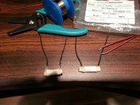
I will post a couple of pics later to help the description. Attached pic was from making the I/V some time ago. You can see the Manganin wire is 110 ohms per foot, so you first calculate the length of wire required for the required resistance. then I remove the enamel from each end by dipping it in a blob of hot solder. Then measure resistance. This stuff is like a very fine piece of human hair so use good tweezers and expect a little trouble seeing. I build the resistor base by taking a small piece of wood (1cm of chop stick) and drill tiny hole in each end. Thread lead out copper wire (24gauge) thru each hole and twist it to be secure on the end of the wood. I then solder the wire where it meets the wood. This further secures it and will be the point where the Manganin attaches to the lead out.
Then wrap double sided sticky tape around the wood. This is the base on which you wrap the wire. Fold the wire in half and start by attaching the center fold of the wireonto the sticky tape and then while holding both pieces of wire between thumb and finger of one hand slowly and carefully twist the resistor with the other hand until the two leads of wire are about 2 cm from the end. This forms a bifilar winding to reduce inductance. In low values like the 60R IV, I doubt there is much problem with 6inches of wire. You can read about low inductance winding on Wiki. I chose bifilar as it is easy and this wire is thin.
Now the truly tricky part. It helps to have a stand with magnifying glass to hold the resistor. you have to carefully attach the wire to the lead out. I find a Q tip with flux on it is the ticket. with the Qtip, tease the wire onto the solder blob. The flux will cause it to stick. Then carefully touch it with a hot iron. with luck the wire is soldered onto the copper lead out. After completing both ends measure resistance. If you have succeeded in attaching the manganin, the proper resistance is achieved. If not an open circuit and you try again.
you want to now ensure there is no movement of the lead out wires at the wood. I use a blob of glue. You also need to be careful not to stress the joint when positioning the resistor, or to reheat the joint. Proper use of plyers to bend the lead out eliminates stress, and then when soldering the leadout to the tub pins hold the lead out with plyers when you touch the soldering iron. The plyers will stop the heat from travelling up the wire to potentially disconnect the manganin.
It sounds like a lot, but the wire is not expensive, and a resistor can be made in 30 mins. They are instantly more transparent, but like everything, I think take a few hours of burnin to fully bloom.
Attachments
Last edited:
Hi Drew
I will post a couple of pics later to help the description. Attached pic was from making the I/V some time ago. You can see the Manganin wire is 110 ohms per foot, so you first calculate the length of wire required for the required resistance. then I remove the enamel from each end by dipping it in a blob of hot solder. Then measure resistance. This stuff is like a very fine piece of human hair so use good tweezers and expect a little trouble seeing. I build the resistor base by taking a small piece of wood (1cm of chop stick) and drill tiny hole in each end. Thread lead out copper wire (24gauge) thru each hole and twist it to be secure on the end of the wood. I then solder the wire where it meets the wood. This further secures it and will be the point where the Manganin attaches to the lead out.
Then wrap double sided sticky tape around the wood. This is the base on which you wrap the wire. Fold the wire in half and start by attaching the center fold of the wireonto the sticky tape and then while holding both pieces of wire between thumb and finger of one hand slowly and carefully twist the resistor with the other hand until the two leads of wire are about 2 cm from the end. This forms a bifilar winding to reduce inductance. In low values like the 60R IV, I doubt there is much problem with 6inches of wire. You can read about low inductance winding on Wiki. I chose bifilar as it is easy and this wire is thin.
Now the truly tricky part. It helps to have a stand with magnifying glass to hold the resistor. you have to carefully attach the wire to the lead out. I find a Q tip with flux on it is the ticket. with the Qtip, tease the wire onto the solder blob. The flux will cause it to stick. Then carefully touch it with a hot iron. with luck the wire is soldered onto the copper lead out. After completing both ends measure resistance. If you have succeeded in attaching the manganin, the proper resistance is achieved. If not an open circuit and you try again.
you want to now ensure there is no movement of the lead out wires at the wood. I use a blob of glue. You also need to be careful not to stress the joint when positioning the resistor, or to reheat the joint. Proper use of plyers to bend the lead out eliminates stress, and then when soldering the leadout to the tub pins hold the lead out with plyers when you touch the soldering iron. The plyers will stop the heat from travelling up the wire to potentially disconnect the manganin.
It sounds like a lot, but the wire is not expensive, and a resistor can be made in 30 mins. They are instantly more transparent, but like everything, I think take a few hours of burnin to fully bloom.
HI wloes. Where do you get manganin wire from?
Hi Eldam,
This schematic might help a bit (attached), you can see that the analog ground pin goes straight to the binary weighted current network. Im pretty sure the return currents for pin 1- 4 will not take this path... as far as my logic can tell.
I wouldn't cut the top plane to pin 5, the power supply return currents will most likely take this path. But don't let me stop you trying. 🙂
Pin 1-4 return currents path should be as follows (from my understanding):
Through the vias around the ufl pads.
Then directly under the trace.
Back up through the vias near pins 1-4.
Under the chip to pin 14.
I think the highest impedance path the currents will encounter will be from the center of the chip to pin 14. (on the top plane, and inside the chip).
The traces for pin 1-4 were calculated to match 50 ohm using Saturn PCB Toolkit V6.64
Thanks Ryan,
I didn't say I want to isolate pin 5 from the upper plane and pin 5 from 14 but isolate pin5 from its near environment (other close vias) by tracing an island to pin 14 (to drive the flow and avoid the other curents 5 V and pin 1 to 4 to return to this pin 5 "before" the pin 14 (as they are tied in each case).
But if you tell me those return currents will see in fact only pin 14... it's ok like it is 🙂. In my mind I believed the return path of those currents drop to the nearest GND pin (as AGND & DGND are tied...). If they know the good path themselves everything is right. I'm not aware about continuous DGND plane with multiple connection to AGND and how it's work really....
Cheers
Last edited:
Luke
Ebay. The vendor is currently offering 200 feet for $16.
200ft 60M E Manganin 46AWG 0 04mm 362 4 ? M 110 ? FT Resistance Wire | eBay
Ebay. The vendor is currently offering 200 feet for $16.
200ft 60M E Manganin 46AWG 0 04mm 362 4 ? M 110 ? FT Resistance Wire | eBay
Hey Eldam,Thanks Ryan,
I didn't say I want to isolate pin 5 from the upper plane and pin 5 from 14 but isolate pin5 from its near environment (other close vias) by tracing an island to pin 14 (to drive the flow and avoid the other curents 5 V and pin 1 to 4 to return to this pin 5 "before" the pin 14 (as they are tied in each case).
But if you tell me those return currents will see in fact only pin 14... it's ok like it is 🙂. In my mind I believed the return path of those currents drop to the nearest GND pin (as AGND & DGND are tied...). If they know the good path themselves everything is right. I'm not aware about continuous DGND plane with multiple connection to AGND and how it's work really....
Cheers
Sorry I misunderstood you.
Ahh, so you mean like a slot in the ground plan to further isolate the analog ground? Thats something that should be looked at further.
After I heard the current design "sound" i was a little nervous to change things too much... "If it ain't broke don't fix it..."
But yeah i see what you mean. All that RF noise so close to the analog ground can't be a good thing.
Maybe a 4 layer PCB is in order...
After I heard the current design "sound" i was a little nervous to change things too much... "If it ain't broke don't fix it..."
Maybe a 4 layer PCB is in order...
While it might be interesting to know if further gains are possible there must also be a point of diminishing return. It is pretty well thought out and certainly sounds great. I suspect the source of a clean signal upstream is the spot to focus now, such as all the interest in clocks, reclocking and isolation.
Ryanj, I did have on question about the design choices. John at ecdesigns was very keen on I2S attenuation. Basically a resistor network on the I2S entry. Was this considered and ruled out in the Distinction design? This certainly would be an easy tweak for someone so inclined using the existing PCB. it would be simple to cut the trace and mount an smt resistor in series with any or all of the I2S traces after the ufl connector. Interested in your thoughts. I am not inclined to change mine, but if one of the truly thorough engineers on the site did the a/b comparison and found a gain, I'd certainly implement it.
ryanj,
With only 11 units on the interest list, do you think there will be a second buy? Any idea on the quantity it will take to make it happen? I would be willing to pay a bit more if needed. Here is the list I bumped up from page 31.
If anybody's interested please put your name on the list and let's make this happen.
Greg Stewart x2
ppap64 x 2
Peterma x 3
kenlaumm x 2
j.burtt x 2
Where can I source TDA1541A non-counterfit chips? Any trustworthy NOS chip suppliers? Sorry for my ignorance, I got two boards from the GB but I know next to nothing about the dac chip availability. Thanks in advance.
Palmito,
I'll trade you a legitimate new old stock TDA1541A for the extra board you have. If this sounds interesting PM me.
James
I'll trade you a legitimate new old stock TDA1541A for the extra board you have. If this sounds interesting PM me.
James
Palmito, I don't remember the name but some members can give you the name of this irish distributor which as some TDA1541A (Rochester hasn't !) yet.
Don't know in the US, but in EU it still possible to source on second hand markett some old Philips/Marantz cd player to keep the TDA inside (for 20 to 40 euros !) : check Vasiltech list to make your markett !
@ Ryan,
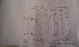
I've done a picture though I didn't want to draw it ! On the picture there is twice the same idea but the left shematic is focused (zoom !).
You see pin 5 is always tied to the plane but on the pin 14 directly via the island and not anymore around itself only by the continuous ground plane . The island is just made by separating it of the upper plane with a scalpel by removing the copper (around the island to draw the path to pin 14) but on the pin 14 of course (as we need to keep them tied: the island touch the upper side of pin 14). Obliquely traces is conductive copper on the picture. Notice also the cut trace from the "island" drawed to the upper edge of the pcb (idem : just a scalpel cut from an edge trace -empty copper- of the "island" to the upper physical edge of the board).
BTW, it's not shown but the cutted trace which start from the pin 5 island to the upper edge of the pcb must be placed between pin 1 to 4 hole chip pins and the three vias holes you added on the board just in front of them as you described already (out path of the return DGND current of pin 1 to 3 (4? is there 4 vias holes ?) to go out on the middle of the plane to flow under the body of the dac chip to pin 14 as you explained!
I'm totaly confused 😱, hope my drawing skill is not worst than my english for your understanding !
Certainly a too naive vision of me (coming from the phrase of T. Loesch : "you must see where the current flows"!) and this story of impedance you talked about is more serious... and we certainly need instruments of simulation with tools we have not to have a valid answer (Marce member : ... mayday 😉).
I hope with the picture one understand the goal is to isolate more (to move away) AGND pin 5 from the too much close pins 1 to 4 and pins 28 & 26 : digital +/- 5 V. To alow the return path Gnd current of pin 1 to 4 and pins 28 & 26 to meet faster pin 14 and just after in second pin 5 but via the island path... With high speed RF, maybe it's important, I just don't know !
Notice also, as the pin 5 is isolated from the close pin 4 : one can add an external MCLK (I asked two vias hole for that : remember ! And they are present). In this scenario : the via hole of the gnd of this clock (near the hole on pin 4 path) is closest to pin 14 as well (instead of pin 5)
regards.
In fact nobody talked about problem with the Distinction-1541 made with the informations we collected in the "any good TDA1541 kit?" thread but asked myself if it was 384 K hz proof for upsampling !
Don't know in the US, but in EU it still possible to source on second hand markett some old Philips/Marantz cd player to keep the TDA inside (for 20 to 40 euros !) : check Vasiltech list to make your markett !
@ Ryan,
I've done a picture though I didn't want to draw it ! On the picture there is twice the same idea but the left shematic is focused (zoom !).
You see pin 5 is always tied to the plane but on the pin 14 directly via the island and not anymore around itself only by the continuous ground plane . The island is just made by separating it of the upper plane with a scalpel by removing the copper (around the island to draw the path to pin 14) but on the pin 14 of course (as we need to keep them tied: the island touch the upper side of pin 14). Obliquely traces is conductive copper on the picture. Notice also the cut trace from the "island" drawed to the upper edge of the pcb (idem : just a scalpel cut from an edge trace -empty copper- of the "island" to the upper physical edge of the board).
BTW, it's not shown but the cutted trace which start from the pin 5 island to the upper edge of the pcb must be placed between pin 1 to 4 hole chip pins and the three vias holes you added on the board just in front of them as you described already (out path of the return DGND current of pin 1 to 3 (4? is there 4 vias holes ?) to go out on the middle of the plane to flow under the body of the dac chip to pin 14 as you explained!
I'm totaly confused 😱, hope my drawing skill is not worst than my english for your understanding !
Certainly a too naive vision of me (coming from the phrase of T. Loesch : "you must see where the current flows"!) and this story of impedance you talked about is more serious... and we certainly need instruments of simulation with tools we have not to have a valid answer (Marce member : ... mayday 😉).
I hope with the picture one understand the goal is to isolate more (to move away) AGND pin 5 from the too much close pins 1 to 4 and pins 28 & 26 : digital +/- 5 V. To alow the return path Gnd current of pin 1 to 4 and pins 28 & 26 to meet faster pin 14 and just after in second pin 5 but via the island path... With high speed RF, maybe it's important, I just don't know !
Notice also, as the pin 5 is isolated from the close pin 4 : one can add an external MCLK (I asked two vias hole for that : remember ! And they are present). In this scenario : the via hole of the gnd of this clock (near the hole on pin 4 path) is closest to pin 14 as well (instead of pin 5)
regards.
In fact nobody talked about problem with the Distinction-1541 made with the informations we collected in the "any good TDA1541 kit?" thread but asked myself if it was 384 K hz proof for upsampling !
Attachments
Last edited:
http://www.diyaudio.com/forums/digi...any-good-tda1541a-dac-kit-36.html#post2887092
T. Loesch inputs about this ground begann from this post.
T. Loesch inputs about this ground begann from this post.
While it might be interesting to know if further gains are possible there must also be a point of diminishing return. It is pretty well thought out and certainly sounds great. I suspect the source of a clean signal upstream is the spot to focus now, such as all the interest in clocks, reclocking and isolation.
Ryanj, I did have on question about the design choices. John at ecdesigns was very keen on I2S attenuation. Basically a resistor network on the I2S entry. Was this considered and ruled out in the Distinction design? This certainly would be an easy tweak for someone so inclined using the existing PCB. it would be simple to cut the trace and mount an smt resistor in series with any or all of the I2S traces after the ufl connector. Interested in your thoughts. I am not inclined to change mine, but if one of the truly thorough engineers on the site did the a/b comparison and found a gain, I'd certainly implement it.
Hi Walter,
Thanks for reminding me, I'm very keen on having a play with attenuating the I2S/PCM. Ill have to have a look at some designs/ideas. I remember seeing it on ECdesigns thread somewhere... Got a link? Or as simple as a series resistor and another resistor going to ground?
The only reason it wasn't included is because i've never experimented with this at all. A few years ago I made up a PCB that used Johns I2S reclocking/attenuation circuit but never ended up populating it... Must have got sidetracked, doesn't take much. 😀
ryanj,
With only 11 units on the interest list, do you think there will be a second buy? Any idea on the quantity it will take to make it happen? I would be willing to pay a bit more if needed. Here is the list I bumped up from page 31.
If anybody's interested please put your name on the list and let's make this happen.
Greg Stewart x2
ppap64 x 2
Peterma x 3
kenlaumm x 2
j.burtt x 2
Im pretty keen on ordering a few soon. I dont think ill wait for x amount on the waiting list. Ill just order 20 or 30.
- Status
- Not open for further replies.
- Home
- Source & Line
- Digital Line Level
- Group buy/Interest list - TDA1541A Core board.