Aah W, we all have a bad day every now and again....
Eldham, I posted a query on the 1541A thread about not understanding your comments about the ground planes and their use as bypass capacitor return tracks - I went back to Ryan's post #303 (photos on this thread) and indeed it appears that the top plane is used as the analogue ground (including the power supplies, etc) and this layer is also connected to the pin 14, and pin 14 underneath is connected to the bottom ground layer but, I don't see any 'cross-connection' anywhere else, unless I'm missing something here.
Perhaps, on the next version of the board, there'll be a separate isolated track (thru the top layer?) between pin 14 and pin 5 to keep the bottom layer, & pin 14, separate from the from the top layer altogether and avoid any possible bypass cross current paths
[Is there a problem in actual use with the top layer tied to analogue ground (pin 5) and the bottom layer tied to the pin 14 'digital' ground? ]
On the present boards, It's relatively easy to separate the top layer from pin 14 (cut copper around pin 14 itself) and run a separate insulated copper wire from pin 14 to pin 5 - easily done.
I don't know how, but we've been remarkably free of any 'agro' on any of the '1541 dac chip' threads for some years now - lets also keep this thread one of the 'really cool' ones ...
Eldam, what are even trying to say. I am struggling to understand anything you type.
I suspect English is not Eldams first language. A more helpful post would be to ask him to clarify his post🙂
Thank you all, WOW all those inputs in one day !
It seems it works better when I leave !
Take your own advice.
This is where i first proposed my pcb for a GB, NOT Eldams design as he has allured to many times in different threads:
This is true, i've been listening to this configuration for quite some time now and am still loving the sound and how well it can differentiate the quality of the albums/recordings. Every time i change the album, the apparent sound of the system changes making it very easy to tell the level of quality of the recording.
Sorry, but I cant offer any distortion measurements, etc. But from what i have learn't along the way i gained the most performance (listening) when I reduced jitter using Ians FIFO. The CEN i/v stage was a good step up from a tube SRPP i/v.
Pretty sure i've uploaded this photo somewhere on another thread but in case anyone is interested and it helps this project in anyway, here it is again. My design goals have been simplicity. Oh and this is a prototype... 2 years and counting.
View attachment 414078
Eldam, even if there is a V2, i will not sell one to you.
I do have plans for a v2, and none of Eldams ramblings will influence the outcome of the PCB, and it didn't for v1. Member likes Marce, setup, ecdesigns, Jameshillj, wlowes, and a few others were a great help. - Eldam is definitely NOT on this list.
Eldam, make your own PCB. I couldn't care less about you at this stage. You are now on my ignore list, so dont bother addressing me in a post, i've had enough of your rambling on. Im sure many others would agree. Your ruining it for everybody, if you keep this up i will not even bother sharing anymore.
Sorry. Long time lurker, first time poster.
After following some of this, and certainly most all of it recently and having had read across multiple threads for some time.
I don't read anywhere that Eldam has claimed the work to be his design (as implicated clearly above), but that he provided some input (whether taken aboard or otherwise) as part of a group, as it clearly was.
In effect, all I see is 'bully boy' tactics, and some 'off the cuff' dismissal remarks from those (in and around and perhaps surrounding) who have a clear commercial interest, or equally egocentric issues, which are simply at odds with Mr Eldams inquisitive nature.
Indeed, if we were to persecute or ex-communivate anyone who had a viewpoint, or question which were at odds with individuals commercial interests or egocentric nature, then what would that make us?.. yet, that is precisely what this has become.
I say pull your head in.
I also find it ironic that some were rebuked in the form of 'don't let it get agro', yet in the end, its come down to some retort from some who cant rise above their own ego and report accurately to the facts. All is based in fear (clearly), yet all Eldam has done is ask, ask and ask again, supporting his reasoning by at the same time asking for validation on his reasoning.
Little boys club.
Indeed he would most likely be better without all of this.
Evolution?. Hardly.
.. and who would buy something from a 'committee' - and thats what you are, who acted like this.
Shame. (on you)
Thanks for your input Kate G.
Your right, Eldam has been helpful in many respects. He seems to know how to get the conversation going. We must be thankful of that.
I apologise for my earlier post, I was too harsh. I must learn to be more tolerating!
Im not claiming to know it all, I certainly do not! Im just here because I want to share my experiences.
This stuff absolutely fascinates me - anything to do with electronics. Lately i've been trying to get my head around all this digital stuff and i feel like im getting somewhere with it, but to be pushed into designing a v2 pcb that is far from being designed is just counter productive, a lot of testing is required - after all, im learning along the way and i hope others are learning from my mistakes and experiences.
The V2 PCB will be developed under its own fruition.
Diyaudio has been a great place for me to learn and make friendships, at times (especially lately, before activity on this thread) a tad on the light side of people sharing their experiences (especially in the Digital line level section) - I decided i want to try and change all this and get a good conversation going. Things were going pretty well.
This recent turn in attitude of this thread is unfortunate, but i think we can get passed it and move on.
Ryan
I too lurk, and I to +1 KateG's comments.Sorry. Long time lurker, first time poster.
Good on yah ryan i appreciate your work for me it was an oppotunity to experiment and gain more understanding with digital inputs thanks mate have tooheys or vb on me!!
Aah W, we all have a bad day every now and again....
Eldham, I posted a query on the 1541A thread about not understanding your comments about the ground planes and their use as bypass capacitor return tracks - I went back to Ryan's post #303 (photos on this thread) and indeed it appears that the top plane is used as the analogue ground (including the power supplies, etc) and this layer is also connected to the pin 14, and pin 14 underneath is connected to the bottom ground layer but, I don't see any 'cross-connection' anywhere else, unless I'm missing something here.
Perhaps, on the next version of the board, there'll be a separate isolated track (thru the top layer?) between pin 14 and pin 5 to keep the bottom layer, & pin 14, separate from the from the top layer altogether and avoid any possible bypass cross current paths
[Is there a problem in actual use with the top layer tied to analogue ground (pin 5) and the bottom layer tied to the pin 14 'digital' ground? ]
On the present boards, It's relatively easy to separate the top layer from pin 14 (cut copper around pin 14 itself) and run a separate insulated copper wire from pin 14 to pin 5 - easily done.
I don't know how, but we've been remarkably free of any 'agro' on any of the '1541 dac chip' threads for some years now - lets also keep this thread one of the 'really cool' ones ...
Thank you James,
the upper side is not clearly only analog one in my understanding as the upper plane is shared with the bottom plane at all the vias for voltage caps (ground leads of each radial caps), also the decoupling of the clocks inputs vias near DATA R path !
Maybe it's fine, I just ask and I'm surprised about some ego reactions here, it's about technic not about people ! In my mind just the upper pin 5 and upper pin 14 must be shared on this upper plane : not the ground main decoupling leads of the caps (not in the same time ! so to me the upper plane is a digital ground aswell as Ryan confired !)
@ Ryan,
If you have the opportunity to read this :
I never claimed it was my design, how it could be possible, I know less than you !
I really don't understand why you take it like that, I didn't said your faulty but ask as usual some improvement by asking ! Your pushed some Rogic and Henk as a disdainful answer... which just pushed me to put right some things : no, not all were coming from you ! Stop, end of the story, no offense from me to you ! Sorry if you take it as an offense !
I don't think it's your design ever, people with good memories remember I was one of the main pusher and conductor of the "any good tda1541 kit" as I trust to the common work... it's not ego from me, I claim from the beginning we are clever all together and should try to make a good board with all the good minds here on diyaudio !
Some of the Distinction1541 are at the opposite of what you said a direct asking of mine, I particulary insist on the uf-l pads iirc ! So the Distinction GB is the result of your help you gave to us to draw, it's a common work and thank you again to you to shared your work with us.
But Mostly it's not an attack against you as you seem to understand it but a Deming wheel for me ! All my asking to you were always friendly if you read it and not an attack ! Some of members help like Marce was a direct asking of me by PM !
In any case you can say I didn't contribute to it ! In any case you can read somewhere I claim this is my design, but without my energy your first batch were yet in the box.
No one can putt of the fact your help was on a first importance, but the same about me !
So, here we are not in the "Any good TDA1541kit" thread; the board becomes your, it's certainly good like that !
Mostly it's your thread, so I will not input here anymore and of course will not ask you for improvement anymore ! I will not ask you as you tell me for a V2. my inputs just came from for what I see on the AYA2 2014 and some others Philips designs !
Thank you Cheung for the AYA2 2014 (and Ceglar with whom you exchange for that) : you probably made the best work to all of us.
regards and sorry fellows for the english
Okay, I see that I missed all those vias on the decoupling caps, etc - perhaps on the next board, or a prototype one, we can try to see if more separation of the upper and lower planes can be achieved so we can try tying each plane into a separate grounding point (ie pin 5 or pin 14) to see if an improvement can be achieved - it's not an immediate thing but could be included with the possible additions to the input attenuators that Ryan is working on now
The inclusion of the Ian's pcm stage produced an obvious improvement in clarity when I heard it a last w/end, so this is clearly a 'step ahead' in the continuing evolution, even tho there's some problems to be sorted yet
It still amazes me that the original design work for this dac chip was carried out over 40 years ago and we're still finding ways to get it to function better - extraordinary really.
Member
Joined 2006
Hi Ryanj and Eldam,
Both of you and among many others in this and the other thread should deserve an applaud, and please not let little things or misunderstanding to hurt our great diy fellowship which we ought to cherish... hey, please look back and see what we went through and have accomplished to date. Joy from lots of fellow diyers from building Ryan's and Pedja's boards yes, around the world!
I say let it go guys and continue the fun and spirit : ) Great to know Ryan is still constantly making improvements on his board, and I also look forward to seeing his v2 to come. : )
Regards,
Cheung
Jameh
If one were able to separate digital from analogue ground plane, I wonder what else might be required to keep the digital noise away from the analogue. Does one need something like a ferrite bead or choke to stop the noise? This is where my lack of formal training hits. It strikes me that these ground paths join somewhere. At the star ground or at least at the earth ground leaving the chassis. Would the noise be present in all the connected ground paths unless it is blocked and allowed to drain.
Must get a scope!
Could not agree more about 1541A.
Ah, my last comment on this thread hopping it helps (maybe) and not having bad words for nothing!
I didn't see it myself when the design was closed:
there are also a lot of micro vias which tie the both side ! the main (maybe) problematics ones are the four micro vias in front of the four to 4 pins for the return of digital ground : near the the pin 5 (agnd), too close maybe .
It could be (maybe) better for a future revision (and also to continue more safetly the experiments and measure on the resistive simutaneous mode) to :
- not tie the pin 5 on the upper side
- stay with the star analog ground on the botom side put tie the pin 14 to it on the bottom side :to tie digital plane(s) to this analog ground (not with pin 5 anymore : this last just see first "analog" signals)
- so the main caps vias for voltage rails could be stay as it is but with cutting their ground via on the upper side (so connected to the digital bottom only ion a v2) : the leads need the bottom side to be soldered !
-then supress (maybe) the direct // smt path of -15 V for the smt // cap which has only a direct path to pin 5 (agnd)
or : drawing path on the bottom side from the decoupling leads of main voltage caps (-/+ 5 V; -15V) to the analog star ground and just removing the upper contact of pin 5 on the upper side.
One could try also on a V2 :
-To cut in two parts the upper plane in the middle of the dac chip aera: so there will be a left upper digital side and an analog upper right side.
-On the bottom side there will be "island paths" to the ground lead of each voltage caps to the analog star ground ! Star ground will be tied on the digital upper left side an the total digital bottom side by the pin 14 via ! Of course upper pin 5 not connected to the upper left digital side !
I use to ask for smt trace for smt ferrite beads for the voltage rails, but it was "refused" !
regards
Eldam,
hope it coul be a technical contribution !
Last edited:
Yes W, couldn't agree more about where the grounds 'join' and not so sure about this 'digital noise' on the chip's performance - I'm certainly no expert either.
However, some of the oft repeated words of AndrewT come back to mind about some of this ground 'stuff' and that's 'where do all the currents flow, both into & out of the chip?' and I've never managed to understand the complete current flow paths, just parts of it, unfortunately, and this to me seems to be more significant that just focusing on slabs of copper in layers called 'ground planes' - I think there's more to it than this, but unable to add any 'words of wisdom'
For example, we have the small input signal currents that trigger the 'input latches (if I've got that right?) and these small currents end up somewhere ...
We have the -2mA externally fed into the output pins 6 & 25, that apparently end up back at the +5V pin 28, complicated by the 1uF cap to the -5V pin 26 (I've never figured out what this is for?)
We have the -15V & -5V supply points doing 'whatever they do' (input stages and all over internal operations) and also the difference between them apparently is indirectly applied to the decoupling caps so I would hazard a guess that these 2 power supply currents end up in both the pin 14 and pin 5 and maybe these complicated pathways work better without the low impedance shunt supplies that we have become happy with.
About the ground layers - I remember the article about ground layer sections and boundaries on the Guido Tent site some time ago and it has stayed in my mind since so Eldham, this could be something that you could have a look at along with adding a couple of those series inductors in the supply lines that you mentioned - I think these will be more/less effective depending on what type of supply is used and not sure that shunt reg would be the best option for all supplies, as you mentioned in post #475 above.
As you mentioned, there's a few of those vias that would make it hard to separate the top/bottom ground layers with this particular board but it could certainly be kept in mind for the next one - the suggestions for a V2 are starting to stack up nicely ....
Again, not being at all that 'clued up' with this ground plane theory, I've tended to ignore it and my rough home designs don't use any at all and the (optional, IMO) bypass caps 'grounds' and such things, seem to be less complicated because I've used the star ground point at pin 5 for the central 0 Volt 'return point' for it all (including pin 14), but not at all sure if this is actually a 'better way' to do it (pin 5 central 0 volt point, that is) - this smaller, neater design is producing such excellent results, let's continue on with just modding it (or suggesting mods) to the current design while Ryan is getting to grips with the pcm signal input arrangements (simultaneous mode inputs)
All good, back on track
All good, back on track
Track to where exactly?.. round and round, and around!! Creating problems that give you something to solve, when they could be avoided completely in the first instance.
Sometimes its better to take advice from those who have offered. The AMR guy who posted here laid it ALL out in black and white - each section, dissected and explained. And his response to the finished design was what? - I'll tell you. WTF??.
Anyway, good to know Eldam has left.
I'll do the same.
Shane
Last edited:
Hi guys,
Thanks James for getting this back on track.
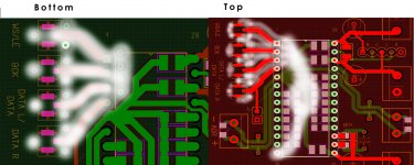
Eldam, im going to try and explain my reasoning for the design of the layout through visual ques - i'd struggle otherwise.
In the picture attached ive drawn how i think the ground "currents" are flowing for the digital signals. Please note that this is more a state of charge than actual current flow when it comes to digital. The fast rising/falling edge of the trace signal is attracting an equal but opposite charge in the area of least impedance (directly underneath the trace - which is why i made the PCB 1.2mm think)
Eldam, from what i understand from your posts, you are worried the analog ground pin should not be connected to near the digital lines? My reasoning to connect the analog ground to the top plane was so the power supply grounds had an uninterrupted path to the analog pin, if this wasn't there they may be faced with some high impedance, creating/emmiting magnetic interferance thus noise.
I hope this is on the right track, maybe someone one out there can fill in the parts i left out.
Please understand that there are defiantly compromises in this layout - as in all designs with only 2 layers, i tried to do it in a way that would work on a 2 layer PCB.
Cheers
Thanks James for getting this back on track.
Eldam, im going to try and explain my reasoning for the design of the layout through visual ques - i'd struggle otherwise.
In the picture attached ive drawn how i think the ground "currents" are flowing for the digital signals. Please note that this is more a state of charge than actual current flow when it comes to digital. The fast rising/falling edge of the trace signal is attracting an equal but opposite charge in the area of least impedance (directly underneath the trace - which is why i made the PCB 1.2mm think)
Eldam, from what i understand from your posts, you are worried the analog ground pin should not be connected to near the digital lines? My reasoning to connect the analog ground to the top plane was so the power supply grounds had an uninterrupted path to the analog pin, if this wasn't there they may be faced with some high impedance, creating/emmiting magnetic interferance thus noise.
I hope this is on the right track, maybe someone one out there can fill in the parts i left out.
Please understand that there are defiantly compromises in this layout - as in all designs with only 2 layers, i tried to do it in a way that would work on a 2 layer PCB.
Cheers
Attachments
Sincere apology to Damien (Eldam)
I believe my actions warrant a much better apology than the one given in a previous post of mine.
I look back on my post and realise what a monster i sounded like, Damien nor anyone deserves this kind of *** hole remark on my behalf. What on earth was going through my head at the time i don't know.
Damien does his very best to better serve this community in his own special way - for this I am grateful as im sure many others are. He has been a valuable and very proactive part of the design process for the Distinction-1541 PCB.
We must remember that this forum contains people from all walks of life, different social statuses, monetary value, etc. We must be more accepting and tolerating. (especially myself). And above all remember that as this is an English speaking forum - for blokes like Damien it may be a bit harder to explain exactly what is in his head due to the translation process.
If Damien could possibly accept my apology for my appalling behavior im sure we can all continue and together produce a Distinction-1541 V2.
Sorry Damien! Your a very valuable member here on diyaudio!!!
sincerest and most apologetic regards,
Ryan
Last edited:
I believe my actions warrant a much better apology than the one given in a previous post of mine.
I look back on my post and realise what a monster i sounded like, Damien nor anyone deserves this kind of *** hole remark on my behalf. What on earth was going through my head at the time i don't know.
Damien does his very best to better serve this community in his own special way - for this I am grateful as im sure many others are. He has been a valuable and very proactive part of the design process for the Distinction-1541 PCB.
We must remember that this forum contains people from all walks of life, different social statuses, monetary value, etc. We must be more accepting and tolerating. (especially myself).
If Damien could possibly accept my apology for my appalling behavior im sure we can all continue and together produce a Distinction-1541 V2.
Sorry Damien! Your a very valuable member here on diyaudio!!!
sincerest and most apologetic regards,
Ryan
Bravo !!!
Not an easy thing to say and full credit to you !!
Shane
- Status
- Not open for further replies.
- Home
- Source & Line
- Digital Line Level
- Group buy/Interest list - TDA1541A Core board.