So nice to see peace on the thread, thanks Kate G, Ryan and Eldam. Can we get back to audio porn already🙂
T The AMR guy who posted here laid it ALL out in black and white - each section, dissected and explained. And his response to the finished design was what? - I'll tell you. WTF??.
Shane
Hi Shane,
Can you please give us a link to where exactly on the thread his dissection was explained? Cheers.
Now.. didn't you have some sheep jokes to share?
Shane, I might get banned and this thread would die, then I wouldn't be able to share distinction V2.0 with you all😀
Hi Shane,
Can you please give us a link to where exactly on the thread his dissection was explained? Cheers.
DIYHiFi.org • View topic - The TDA1541 PCB project at the Pub...
Hi Shane,
Can you please give us a link to where exactly on the thread his dissection was explained? Cheers.
http://www.diyaudio.com/forums/digital- ... it-36.html
Shane, I might get banned and this thread would die, then I wouldn't be able to share distinction V2.0 with you all😀
Use the Force, Luke.
Bravo !!!
Not an easy thing to say and full credit to you !!
Shane
+1
...it's important in life to try staying a just man.
PS: mathematic & number are easier to understand, hopping Ryan & Montgomery can read it.
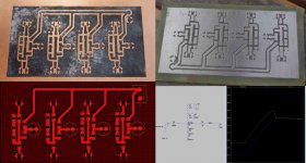
Attenuation update.
Hi Everyone,
Just wanted to share where i'm at with the atten stuff.
R1 and R2 are not 470R as in the schematics, it simulates better having them 750R each. puts a bit less strain on the logic driving chip at the other end.(Iancanada i2s to pcm pcb). Also R3 may be omitted or 10R, just going to try and see how it sounds, gives less overshoot with a small amount of series resistance.
Vias (drilled hole in this case) will be drilled to connect both copper fill layers to follow some type of digital design protocols - A bit of rough impedance matching. Im using this pcb as function verification only- not expecting amazing results. If it works it could be included into future designs, have to test it first.
Happy Easter/Equinox!
Cheers.
Attachments

Last edited:
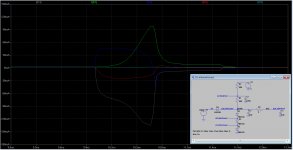
Circuit simulated current flow
Attached is the simulated current flow on the rising edge going through the attenuation circuit. Really helps to understand what is actually going on here.
Parts for the circuit have been ordered, once arrived ill finish the pcb and start testing. After the test period we will know whether its worth pursuing or not.
Id like for the members on the current list to note next to their name whether they want a V1 or wait for a V2.
Eg:
Johnson x1 V2
Gareth x2 V1
Cheers
Attachments
Good on yah ryan i appreciate your work for me it was an oppotunity to experiment and gain more understanding with digital inputs thanks mate have tooheys or vb on me!!
Thanks Peterma, missed your post.🙂
Greg Stewart x2
ppap64 x 2
Peterma x 3
kenlaumm x 2
j.burtt x 2
crowlie x3 V2
ed linssen x1
mravinsky x2 V2
ppap64 x 2
Peterma x 3
kenlaumm x 2
j.burtt x 2
crowlie x3 V2
ed linssen x1
mravinsky x2 V2
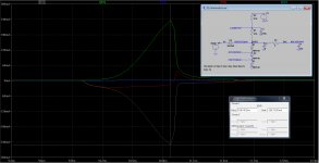
Comparison
Attached a screenshot:
Same circuit, a few different values
R1, R2 now 470R not 680R
C3 now 0pF not 22pF
If you look at the current of D4, it is close to exceeding the max recomended latch up current in the potato logic datasheet. This is why the change in values seemed necessary.
Attached a screenshot:
Same circuit, a few different values
R1, R2 now 470R not 680R
C3 now 0pF not 22pF
If you look at the current of D4, it is close to exceeding the max recomended latch up current in the potato logic datasheet. This is why the change in values seemed necessary.
Attachments
Greg Stewart x2
ppap64 x 2
Peterma x 3
kenlaumm x 2 V2
j.burtt x 2
crowlie x3 V2
ed linssen x1
mravinsky x2 V2
ppap64 x 2
Peterma x 3
kenlaumm x 2 V2
j.burtt x 2
crowlie x3 V2
ed linssen x1
mravinsky x2 V2
Greg Stewart x2
ppap64 x 2
Peterma x 3
kenlaumm x 2 V2
j.burtt x 2
crowlie x3 V2
ed linssen x1
mravinsky x2 V2
palmito x2 V2
ppap64 x 2
Peterma x 3
kenlaumm x 2 V2
j.burtt x 2
crowlie x3 V2
ed linssen x1
mravinsky x2 V2
palmito x2 V2
Greg Stewart x2
ppap64 x 2
Peterma x 3
kenlaumm x 2 V2
j.burtt x 2
crowlie x3 V2
ed linssen x1 V2
mravinsky x2 V2
palmito x2 V2
ppap64 x 2
Peterma x 3
kenlaumm x 2 V2
j.burtt x 2
crowlie x3 V2
ed linssen x1 V2
mravinsky x2 V2
palmito x2 V2
- Status
- Not open for further replies.
- Home
- Source & Line
- Digital Line Level
- Group buy/Interest list - TDA1541A Core board.